Nitride-based light-emitting device

a technology of nitride and light-emitting devices, which is applied in the direction of semiconductor/solid-state device manufacturing, semiconductor devices, electrical apparatus, etc., can solve the problems of inability to increase manufacturing efficiency, inability to reduce dislocation density, and affect the quality of conventional nitride-based light-emitting devices

Inactive Publication Date: 2014-01-16
EPISTAR CORP
View PDF28 Cites 8 Cited by
  • Summary
  • Abstract
  • Description
  • Claims
  • Application Information

AI Technical Summary

Benefits of technology

[0007]A detailed description is given in the following embodiments with reference to the accompanying drawings. An embodiment of a nitride-based light-emitting device is provided. The nitride-based light-emitting device comprises a substrate, a nitride-based buffer layer, a first nitride-based semiconductor layer, a light-emitting layer, and a second nitride-based semiconductor layer. The nitride-based buffer layer is formed over the substrate by nitrogen and at least a first group III element while a second group III element is optionally included. When the second group III element is presented, the concentrations of the first group III element, the second group III element, and nitrogen add up to one. The portion of the nitride-based buffer layer close to the substrate has higher concentration of the first group III element than that of the second group III element, and the combined concentration of the first group III element and the second group III element is greater than that of nitrogen. The portion of the nitride-based buffer layer away from the substrate has a lower concentration of the first group III element than that of the second group III element. In addition, the nitride-based buffer layer has lower nitrogen concentration close to the substrate and higher nitrogen concentration away from the substrate. The first nitride-based semiconductor layer is formed over the nitride-based buffer layer. The light-emitting layer is formed over the first nitride-based semiconductor layer, and the second nitride-based semiconductor layer is formed over the light-emitting layer.

Problems solved by technology

Due to the mismatching of the crystal lattice constants, the dislocation density (which affects the quality of the conventional nitride-based light-emitting device) cannot be decreased efficiently.
The thickness and temperature of the buffer layer, the recovery of the heating and re-crystallization processes, plus the ratio and flow rate of gas for each reaction must be controlled precisely, thus the manufacturing process becomes complicated and difficult, and the manufacturing efficiency cannot be increased.

Method used


Image

  • Nitride-based light-emitting device
  • Nitride-based light-emitting device
  • Nitride-based light-emitting device

Examples


first embodiment

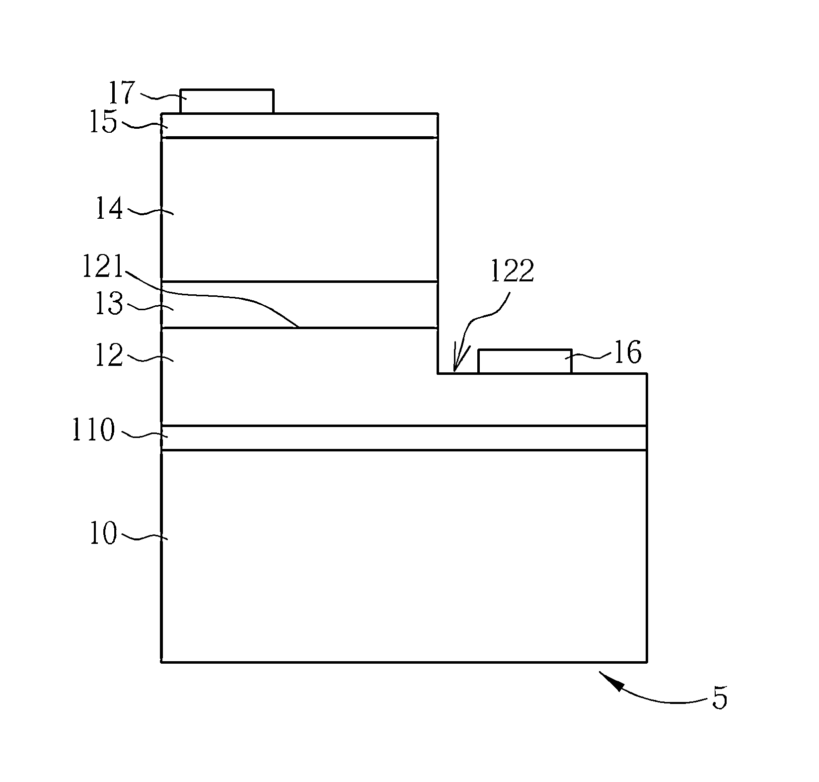
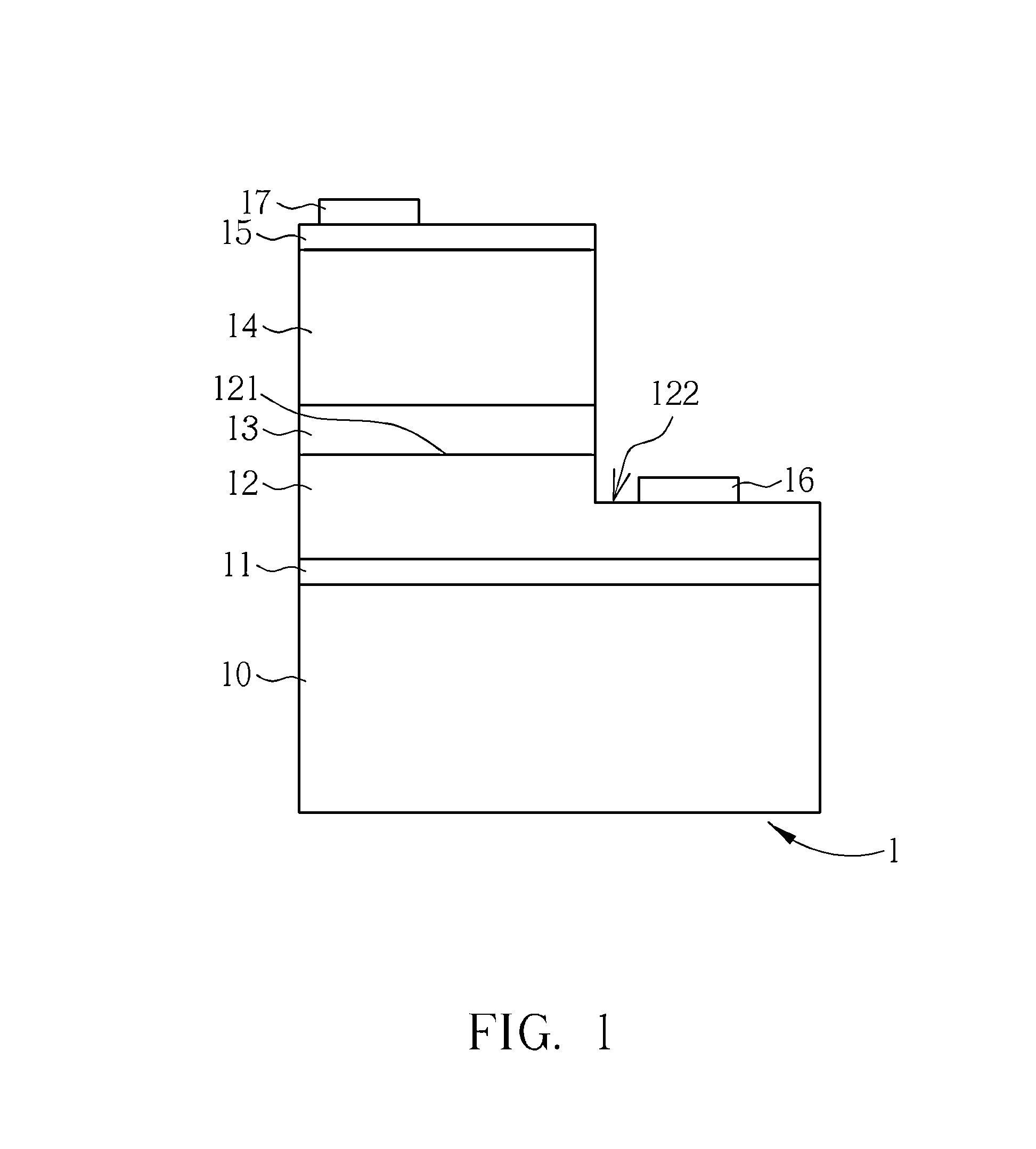
[0020]Please refer to FIG. 1, which illustrates a schematic diagram of a nitride-based light-emitting device 1 with an AlGaN buffer layer according to the present disclosure. The nitride-based light-emitting device 1 includes a sapphire substrate 10, an AlGaN buffer layer 11 formed over the sapphire substrate 10, a nitride-based stack layer 12 made of n-type semiconductor and formed over the AlGaN buffer layer 11 with an epitaxy area 121 and an n-type electrode contact area 122, a multi-quantum well light-emitting layer 13 made of nitride materials like GaN / InGaN formed over the epitaxy area 121, a nitride-based stack layer 14 made of p-type semiconductor and formed over the multi-quantum well light-emitting layer 13, a metal transparent conductive layer 15 formed over the nitride-based stack layer 14, an n-type electrode 16 formed over the n-type electrode contact area 122, and a p-type electrode 17 formed over the metal transparent conductive layer 15.

[0021]A method for forming th...

fourth embodiment

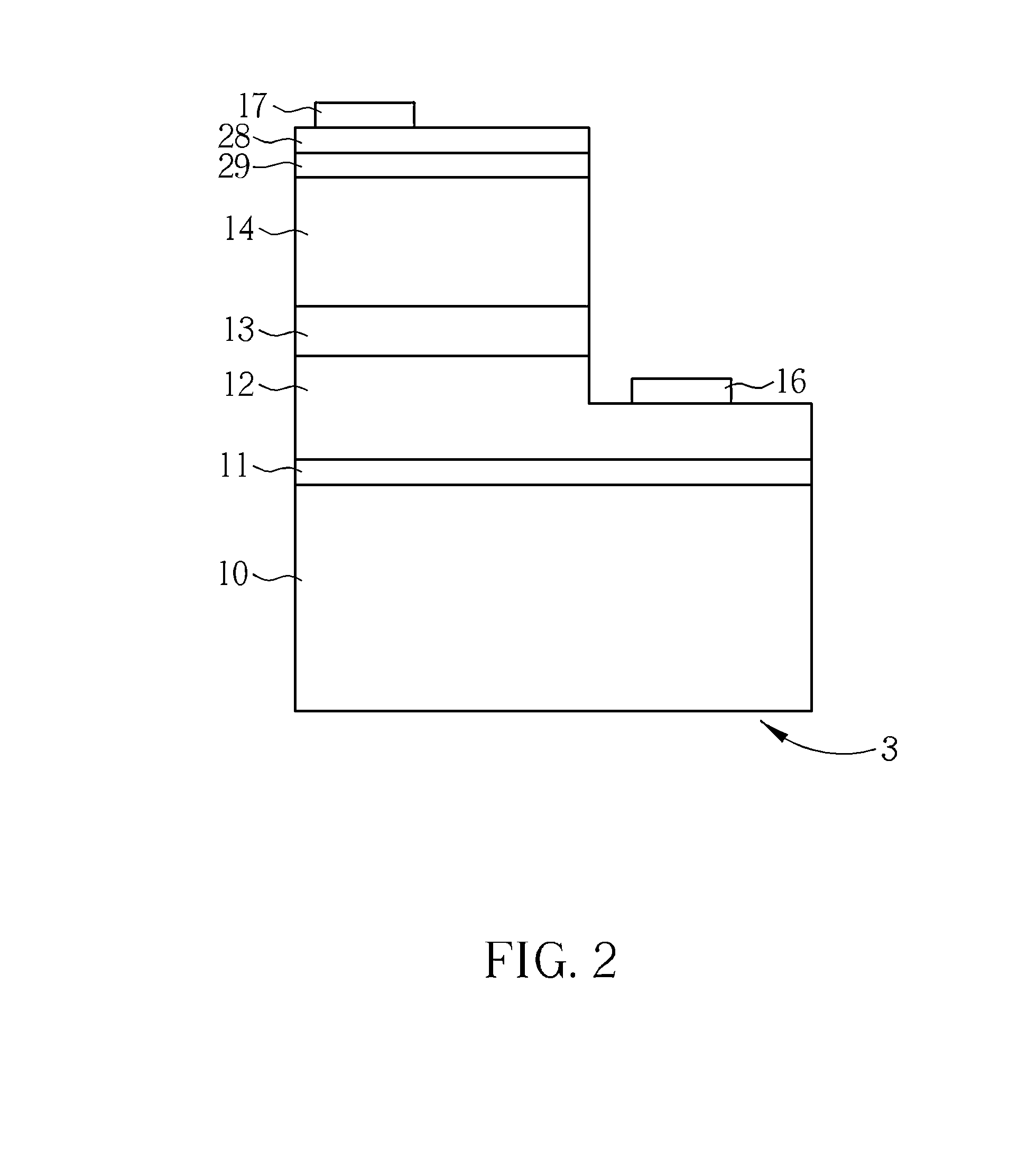
[0080]Please refer to FIG. 11, which illustrates a schematic diagram of a nitride-based light-emitting device 7 with an AlN buffer layer according to the present disclosure. The structure of the nitride-based light-emitting device 7 is the same as the nitride-based light-emitting device 3. The difference between the nitride-based light-emitting device 3 and the nitride-based light-emitting device 7 includes the material of the buffer layer 11 of the nitride-based light-emitting device 7 is AlN.

[0081]In addition, the AlN buffer layers of the nitride-based light-emitting devices 5 and 7 can be replaced with other binary nitride-based buffer layers, such as GaN or InN buffer layer.

[0082]In the nitride-based light-emitting devices 1 and 5, a transparent oxide contact layer can be formed over the nitride-based stack layer instead of the metal transparent conductive layer of the nitride-based light-emitting device 1 for increasing light-emitting efficiency owing to the higher light transm...


PUM


Abstract

A nitride-based light-emitting device includes a substrate and a plurality of layers formed over the substrate in the following sequence: a nitride-based buffer layer formed by nitrogen, a first group III element, and optionally, a second group III element, a first nitride-based semiconductor layer, a light-emitting layer, and a second nitride-based semiconductor layer.

Description

CROSS REFERENCE TO RELATED APPLICATIONS[0001]The present application is a continuation-in-part application of U.S. patent application Ser. No. 13 / 776,312, filed on Feb. 25, 2013, now pending, which is a continuation-in-part application of U.S. patent application Ser. No. 13 / 046,490, filed on Mar. 11, 2011, now pending, which is a divisional of a U.S. Pat. No. 7,928,424, issued Apr. 19, 2011, which is a continuation-in-part of a U.S. Pat. No. 7,497,905, issued Mar. 3, 2009, and which claims the right of priority based on Taiwan Application Serial Number 093106415, filed Mar. 11, 2004, the disclosure of which is incorporated herein by reference in their entireties.BACKGROUND OF THE DISCLOSURE[0002]1. Technical Field[0003]The present disclosure provides a nitride-based light-emitting device, especially a nitride-based light-emitting device including a nitride-based buffer layer.[0004]2. Description of the Related Art[0005]The applications of light-emitting diodes are extensive, such as...

Claims


Application Information

Patent Timeline
Patent Type & Authority Applications(United States)
IPC IPC(8): H01L33/00
CPCH01L33/0075H01L21/0237H01L21/0242H01L21/02458H01L21/0254H01L21/0262H01L33/007H01L33/12
Inventor OU, CHENLIN, WEN-HSIANGLAI, SHIH-KUO
Owner EPISTAR CORP
Why Eureka
Try Eureka