
Method for fabricating a metal-insulator-metal capacitor

Active Publication Date: 2014-01-16
BAE SYST INFORMATION & ELECTRONICS SYST INTERGRATION INC
View PDF5 Cites 1 Cited by
  • Summary
  • Abstract
  • Description
  • Claims
  • Application Information

AI Technical Summary

Benefits of technology

The present invention provides a method for creating a structure with a plurality of metal layers and insulator layers. The method includes depositing a nitride layer on top of a first metal layer, etching the nitride layer and the first metal layer to form a metal-insulator-metal capacitor (MIMCap) metal layer, and filling the gaps between the metal layers with plasma oxide. The excess plasma oxide is polished using the nitride layer as a polish stop. A dielectric layer and a second metal layer are then deposited on the MIMCap metal layer. Finally, the dielectric layer and the second metal layer are etched to form a set of MIMCap structures. The technical effects include creating a structure with multiple layers of metal and insulator layers, and a method for filling the gaps between them using plasma oxide and nitride layer polishing.

Problems solved by technology

As a result, defects are allowed to form since the upper levels are patterned and etched first, which makes the wafer non-planar and much more difficult for the lowest (i.e., the most critical) metal layer to be patterned.
Also, defects formed during the patterning of the upper metal layer can cause defects on the lower metal layer due to micromasking.

Method used


Image

  • Method for fabricating a metal-insulator-metal capacitor
  • Method for fabricating a metal-insulator-metal capacitor
  • Method for fabricating a metal-insulator-metal capacitor

Examples


Embodiment Construction

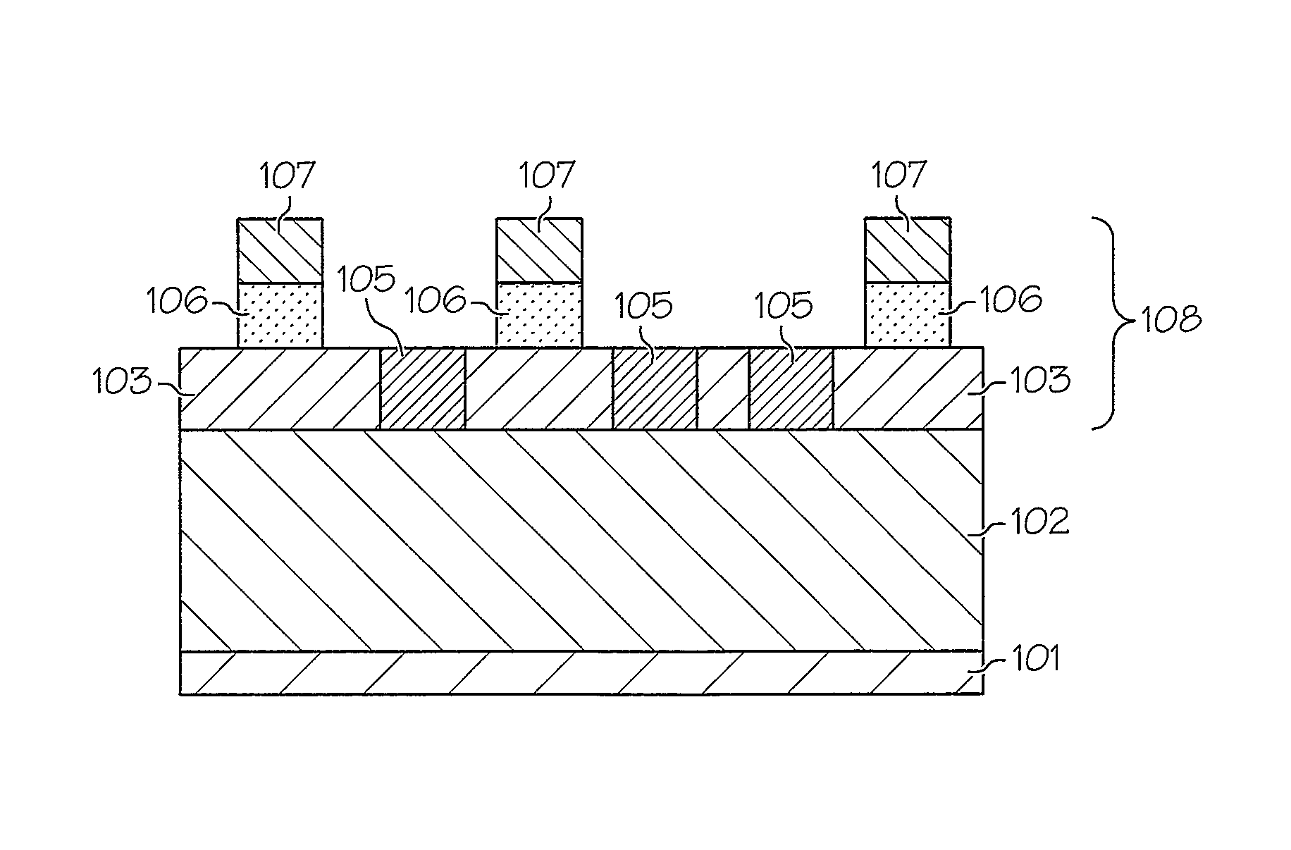
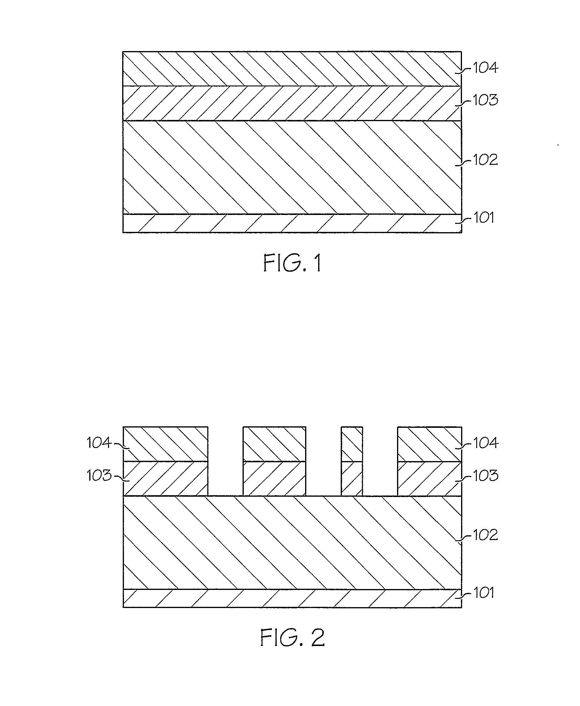
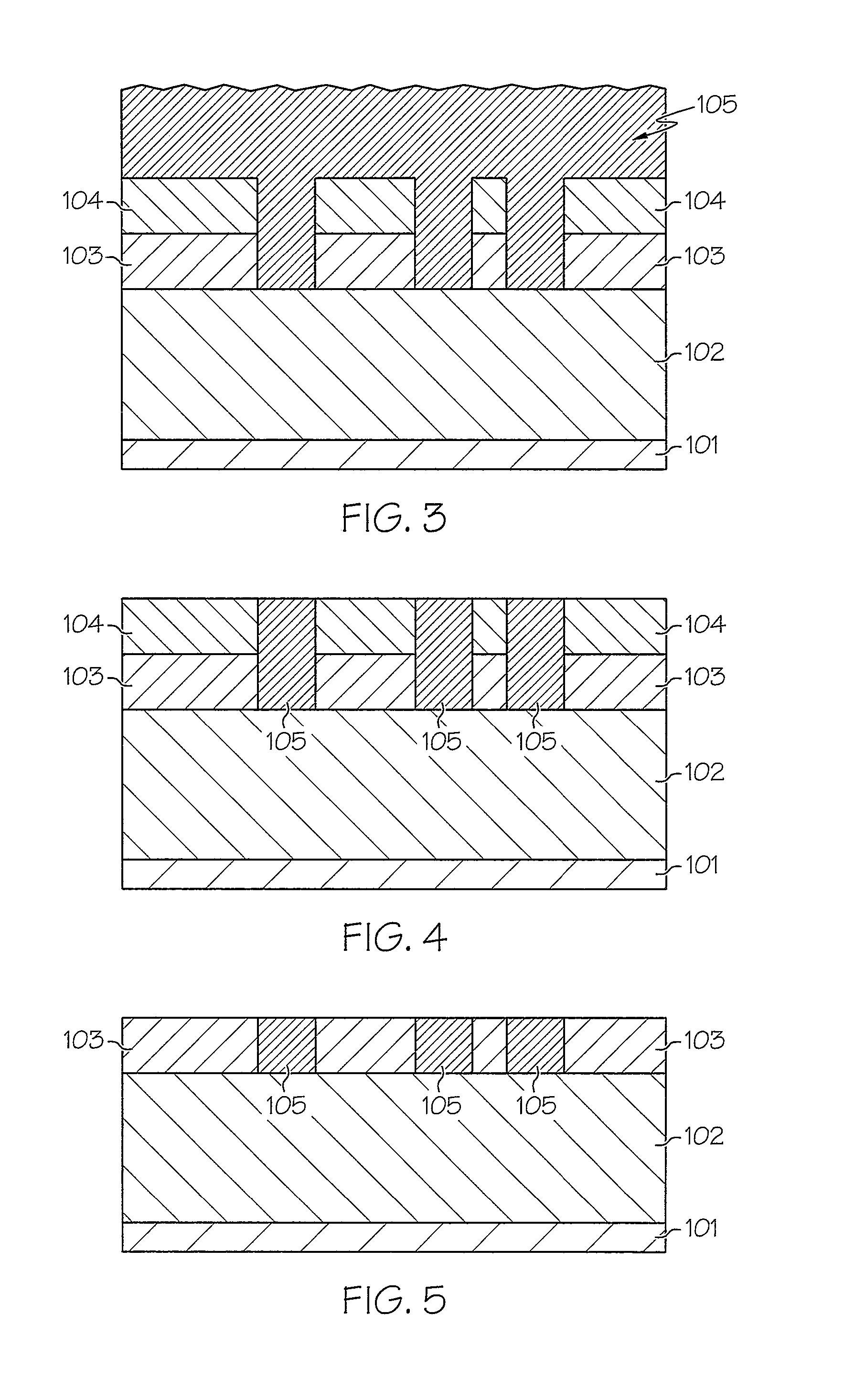
[0012]Referring now to the drawings and in particular to FIG. 1, there is illustrated a method for fabricating a metal-insulator-metal capacitor (MIMCap), in accordance with a preferred embodiment of the present invention. The process begins with an initial structure having a silicon substrate 101, a buried oxide (BOX) layer 102, a metal layer 103 and a nitride layer 104, as shown in FIG. 1. Metal layer 103 is preferably a stack of titanium / titanium nitride / aluminum copper / titanium / titanium nitride with titanium nitride being the top layer. For example, metal layer 103 may include 150 Å Ti, 200 Å TiN, 4,000 Å AlCu, 44 Å Ti and 375 Å TiN. Nitride layer 104, which is approximately 300 Å thick, can be silicon nitride (Si3N4) or silicon oxynitride (SiOxNx).

[0013]A photoresist layer is then placed on top of nitride layer 104 to etch metal layer 103. After the etching has been completed and the photoresist layer has been removed, metal layer 103 is fully patterned, as shown in FIG. 2.

[001...


PUM


Abstract

A method for fabricating a metal-insulator-metal capacitor (MIMCap) is disclosed. A first metal layer is provided on top of an oxide layer. A nitride layer is then deposited on the first metal layer. The nitride layer and the first metal layer are etched to form a MIMCap metal layer. The gaps among the MIMCap metal layer are filled with a plasma oxide, and the excess plasma oxide is polished using the nitride layer a polish stop. After removing the nitride layer, a dielectric layer and a second metal layer are deposited on the MIMCap metal layer. Finally, the dielectric layer and the second metal layer are etched to form a set of MIMCap structures.

Description

BACKGROUND OF THE INVENTION[0001]1. Technical Field[0002]The present invention relates to semiconductor devices having a stacked metal-insulator-metal capacitor in general, and in particular to a method for fabricating a stacked metal-insulator-metal capacitor.[0003]2. Description of Related Art[0004]As the size of integrated circuits becomes smaller and smaller, capacitors used in memory storage cells need to have a higher capacitance per unit area. One technique of increasing capacitance per unit area is by changing capacitors from their typical polysilicon-insulator-polysilicon configuration to a metal-insulator-metal (MIM) configuration.[0005]A metal-insulator-metal capacitor (MIMCap) is a specific type of capacitor having a dielectric layer embedded within two metal plates that are parallel to a semiconductor wafer surface. The MIMCap process flow typically contains a metal stack / cap oxide / metal stack integrated into a back-end-of-the-line (BEOL) structure. In addition to highe...

Claims


Application Information

Patent Timeline
IPC IPC(8): H01L21/02
CPCH01L23/5223H01L28/60H01L2924/0002H01L2924/00
Inventor ROSS, JASON F.YANG, CHI-HUAMCINTYRE, THOMAS J.
Owner BAE SYST INFORMATION & ELECTRONICS SYST INTERGRATION INC
Learn More