Multilayered ceramic electronic component and manufacturing method of the same

a technology of ceramic electronic components and manufacturing methods, applied in the direction of fixed capacitor details, stacked capacitors, fixed capacitors, etc., can solve the problems of deterioration reliability, non-uniform shape of solder layers, and serious concern for heat generation, so as to prevent crack generation, improve reliability, and reduce plating time

Inactive Publication Date: 2014-01-23
SAMSUNG ELECTRO MECHANICS CO LTD
View PDF0 Cites 8 Cited by
  • Summary
  • Abstract
  • Description
  • Claims
  • Application Information

AI Technical Summary

Benefits of technology

[0020]An aspect of the present invention provides a multilayered ceramic electronic component capable of preventing crack generation at the time of soldering a multilayered ceramic electronic component on a PCB, or the like, to thereby improve reliability thereof and reduce a plating time at the time of forming external electrodes.

Problems solved by technology

Due to the recent trend for large-sized display devices, a central processing unit (CPU) therein is increased in terms of a speed, and the like, and so heat generation becomes a serious concern.
However, at the time of forming two or more kinds of solder layers for mounting on PCB, or the like, the glass has a lower wetting level than that of copper, resulting in a solder layer having a non-uniform shape being formed.
In addition, a separation phenomenon, or cracks, and the like, may occur due to the above-described phenomenon, at the time of being mounted on a PCB, such that a plating solution may be permeated therethrough to deteriorate reliability and increase a plating time.
Meanwhile, in order to solve this problem, in the case in which glass material is removed from the surface of the external electrode or an added amount thereof is decreased, adhesive force between the ceramic body and the external electrode itself is offset, such that the shapes thereof are not maintained to be uniform, or the adhesive force therebetween is deteriorated, such that reliability may be degraded.
However, in the following Related Art Documents, Patent Document 1 does not disclose that first and second conductive layers are glass-free.
In addition, since Patent Document 2 discloses a first external electrode including glass, it may be difficult to solve the problem of deterioration of reliability through the implementation of the invention thereof.

Method used


Image

  • Multilayered ceramic electronic component and manufacturing method of the same
  • Multilayered ceramic electronic component and manufacturing method of the same
  • Multilayered ceramic electronic component and manufacturing method of the same

Examples


Embodiment Construction

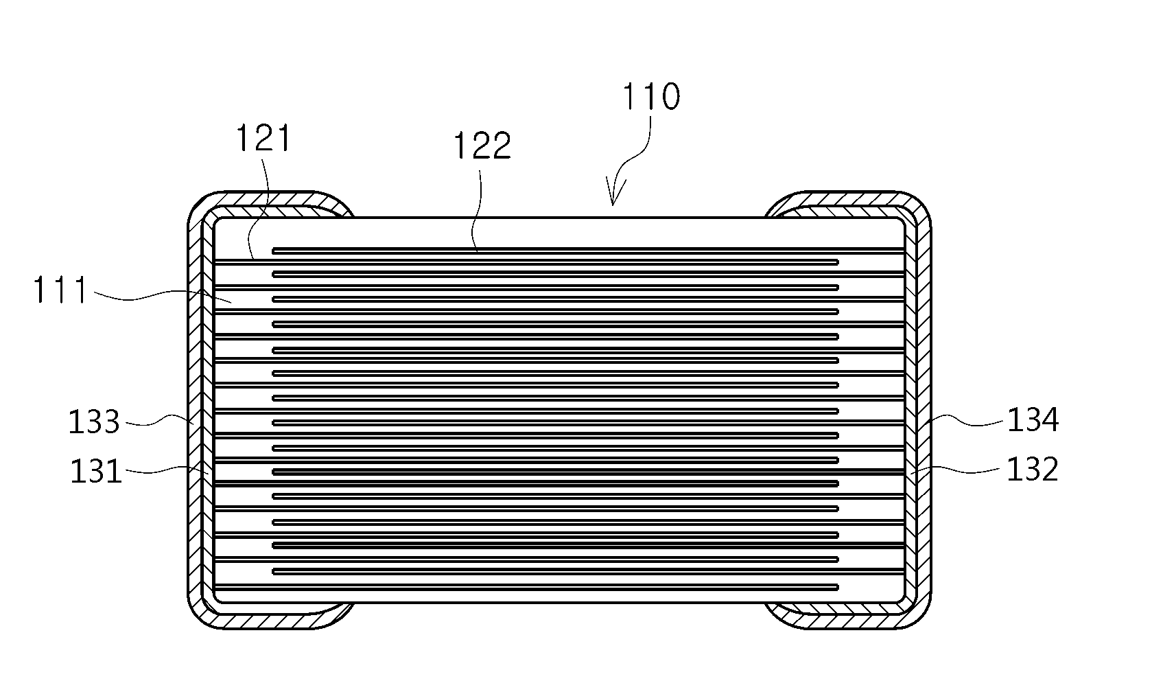
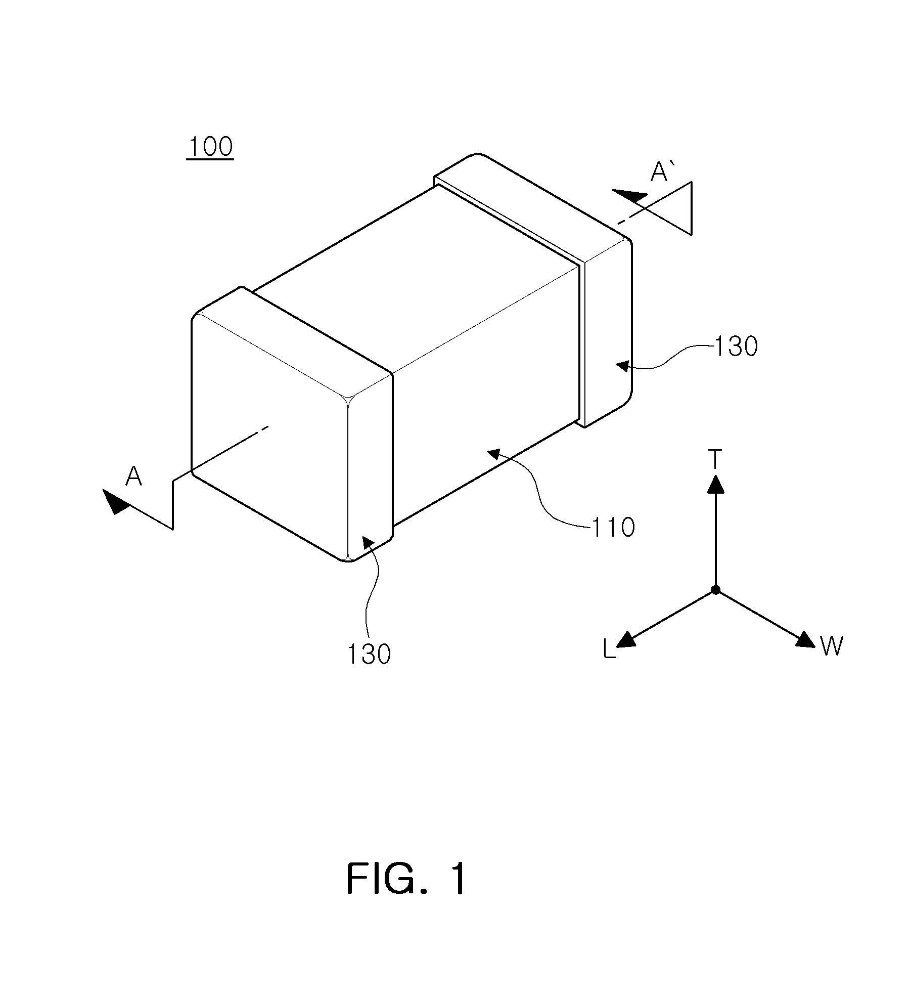
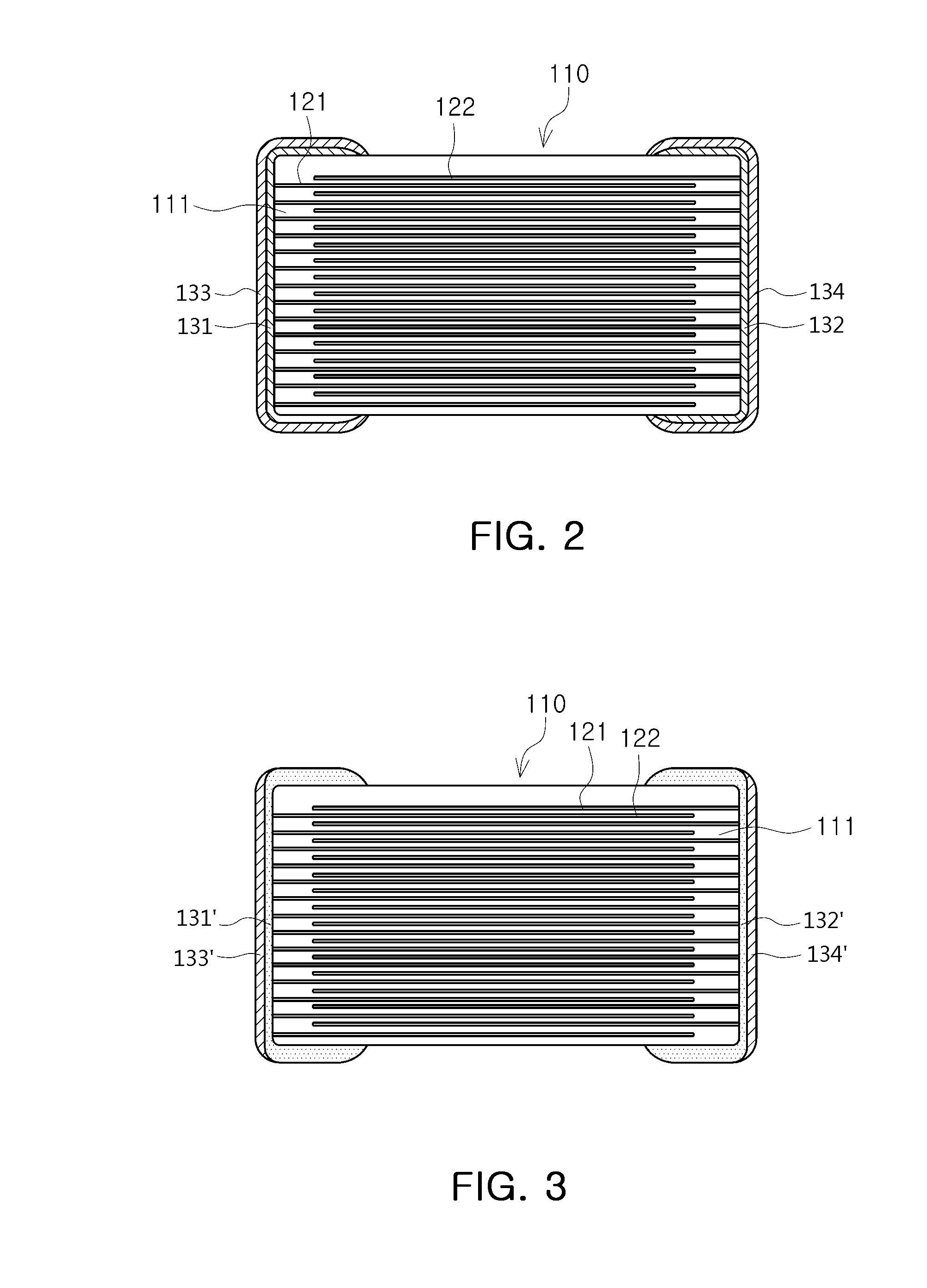
[0037]Hereinafter, embodiments of the present invention will be described in detail with reference to the accompanying drawings. The invention may, however, be embodied in many different forms and should not be construed as being limited to the embodiments set forth herein. Rather, these embodiments are provided so that this disclosure will be thorough and complete, and will fully convey the scope of the invention to those skilled in the art.

[0038]In the drawings, the shapes and dimensions of elements may be exaggerated for clarity, and the same reference numerals will be used throughout to designate the same or like elements.

[0039]In addition, unless explicitly described otherwise, “comprising” any components will be understood to imply the inclusion of other components but not the exclusion of any other components.

[0040]According to an embodiment of the present invention, a multilayered ceramic electronic component is provided. As an example of the multilayered ceramic electronic ...


PUM

PropertyMeasurementUnit
sizeaaaaaaaaaa
particle diameteraaaaaaaaaa

Abstract

There is provided a multilayered ceramic electronic component including: a ceramic body in which a plurality of dielectric layers are multilayered; a plurality of first and second internal electrode layers formed on at least one surfaces of the dielectric layers and alternately exposed through both ends of the ceramic body in a length direction thereof; first and second adhesive layers formed on both ends of the ceramic body, electrically connected the exposed first and second internal electrodes and formed of a conductive paste; and first and second external electrode layers formed on surfaces of the first and second adhesive layers and formed of a glass-free conductive paste.

Description

CROSS-REFERENCE TO RELATED APPLICATIONS[0001]This application claims the priority of Korean Patent Application No. 10-2012-0078849 filed on Jul. 19, 2012, in the Korean Intellectual Property Office, the disclosure of which is incorporated herein by reference.BACKGROUND OF THE INVENTION[0002]1. Field of the Invention[0003]The present invention relates to a multilayered ceramic electronic component and a manufacturing method of the same.[0004]2. Description of the Related Art[0005]As examples of electronic components using a ceramic material, there may be provided a capacitor, an inductor, a piezoelectric element, a varistor, a thermistor, and the like.[0006]Among the ceramic electronic components, a multilayered ceramic capacitor (MLCC) has a small size and high capacity secured therein, and is easily mounted.[0007]A multilayered ceramic capacitor, a chip condenser having a chip shape, is installed in circuit boards of various electronic products including a display device such as a ...

Claims


Application Information

Patent Timeline
Patent Type & Authority Applications(United States)
IPC IPC(8): H01G4/30
CPCH01G4/30H01G4/12H01G4/1227H01G4/2325
Inventor KWAG, JOON HWANKIM, SANG HUK
Owner SAMSUNG ELECTRO MECHANICS CO LTD
Why Eureka
Try Eureka