
Integrated-circuit switch

a switch and integrated circuit technology, applied in the field of switches, can solve the problems of high cost, difficult to carry out circuit customization, complicated circuit design or customization, etc., and achieve the effect of increasing the heat dissipation area and easy application

Inactive Publication Date: 2014-02-13
MESTK INNOVATION
View PDF3 Cites 3 Cited by
  • Summary
  • Abstract
  • Description
  • Claims
  • Application Information

AI Technical Summary

Benefits of technology

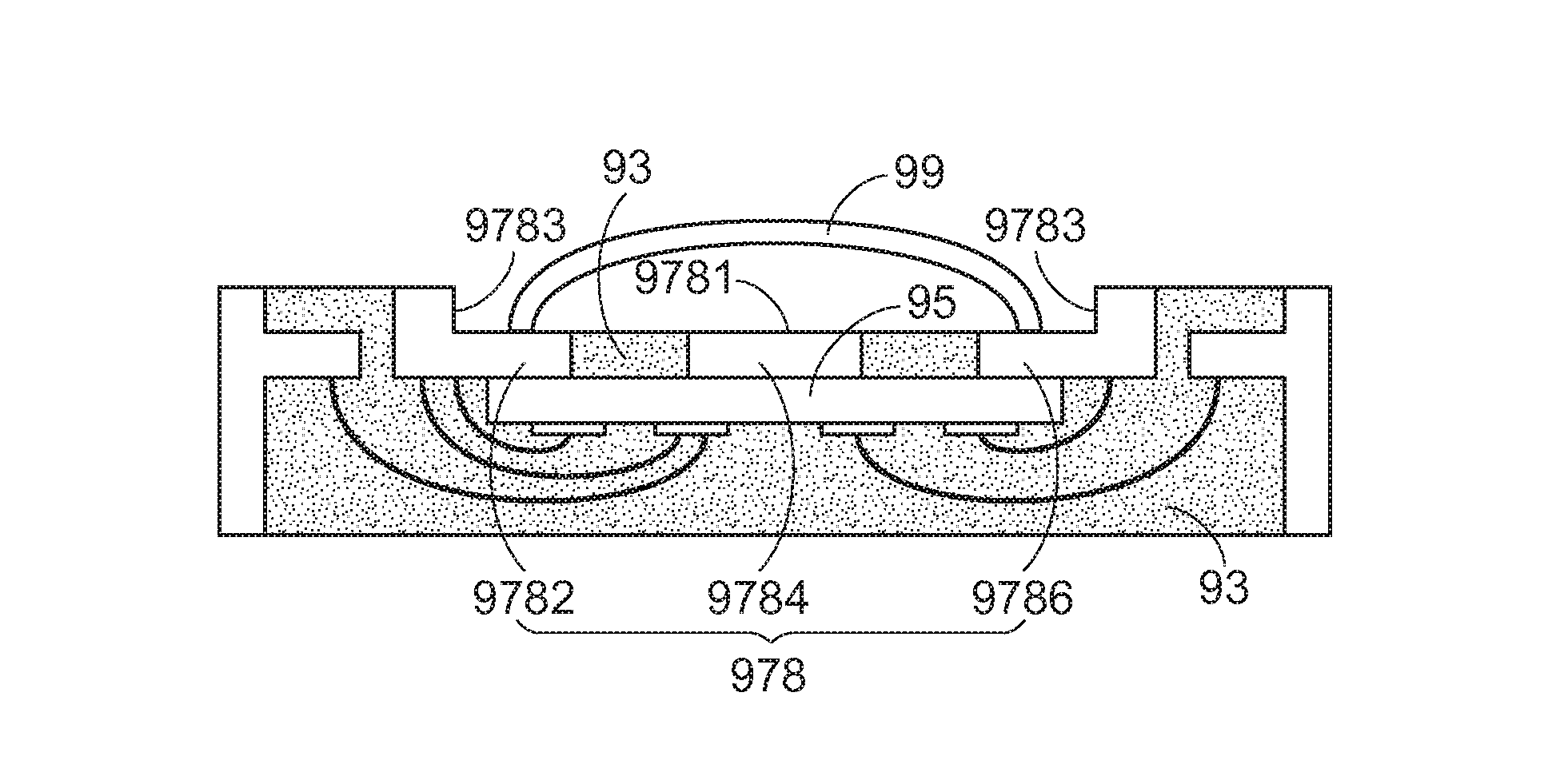
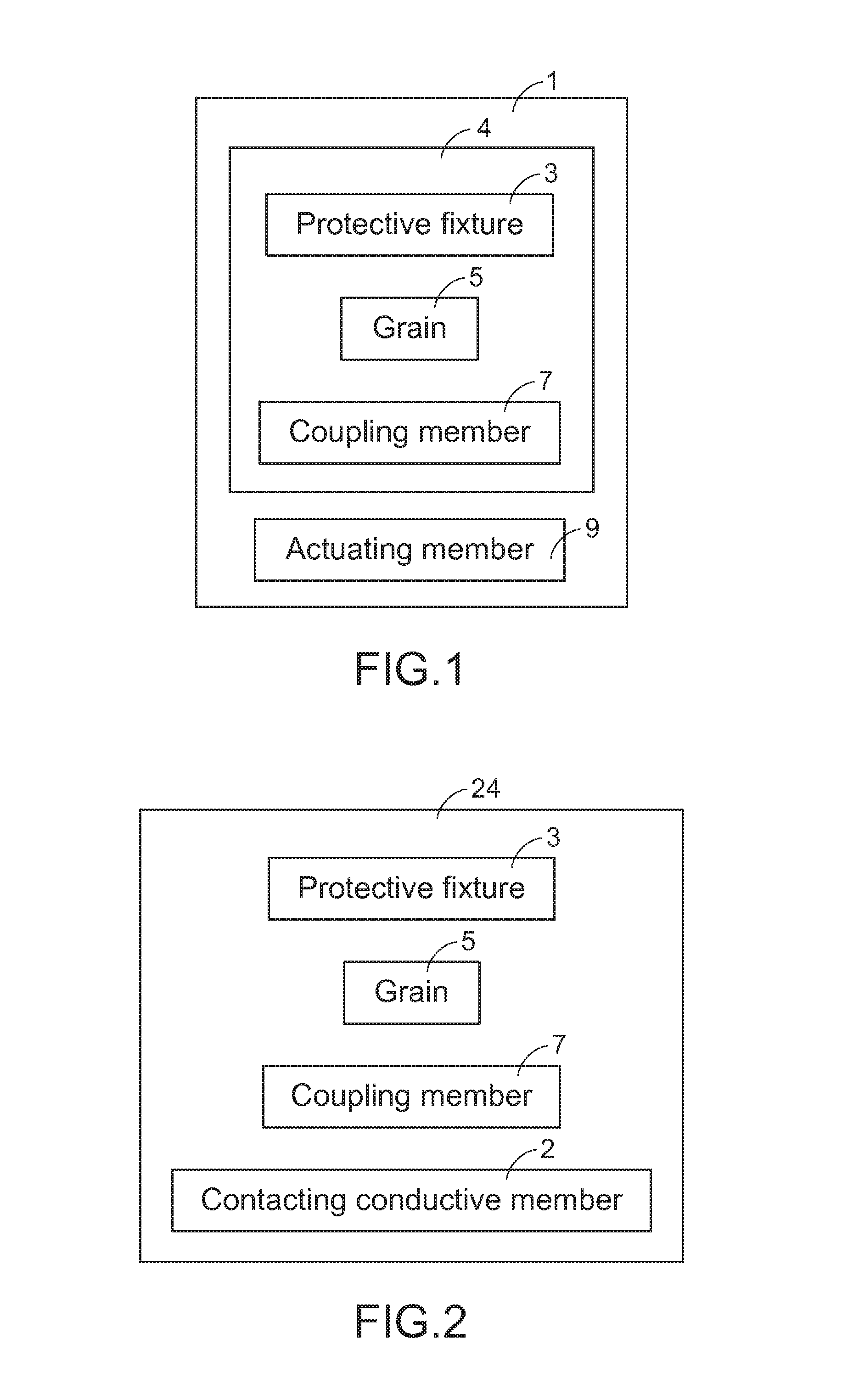
The invention combines a mechanical switch and a grain to efficiently activate the switch when it comes in contact with a bonding surface. This makes it easy to use the switch and suitable for high voltage and current. The switch's actuating structure is formed on the packaging structure, which also serves as a heat dissipating member to increase heat dissipation.

Problems solved by technology

However, while a user applied the electrical switch in the application system with high voltage or high current, here comes the drawback that the cost is high, or the circuit is customized with complicated design or hard to be carried out.
Moreover, a problem is generated that the volume of the electrical switch circuit is too big.

Method used


Image

  • Integrated-circuit switch
  • Integrated-circuit switch
  • Integrated-circuit switch

Examples


first embodiment

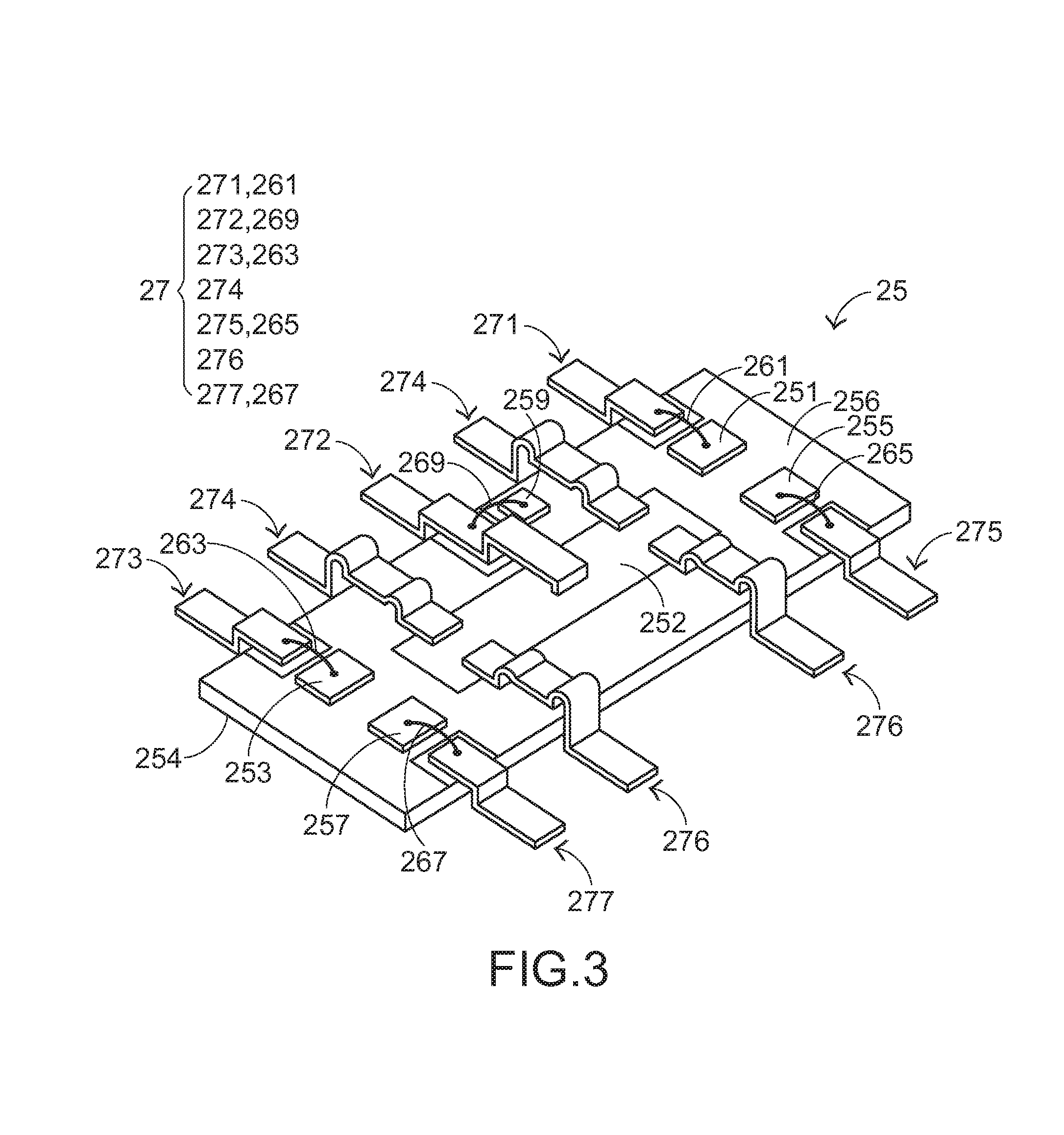
[0054]In more detail, the grain 25 has an electrical insulating first surface 254 (back side) opposite to a second surface (active surface), and the grain 25 has a plurality of pads 251, 252, 253, 255, 257, 259 disposed on the second surface 256 for used to input or output physical signal. In the first embodiment, the conductive pad 252 is disposed on a center region of the second surface 256, pads 251, 253, 255, 257, 259 are arranged around the pad 252 on the second surface with intervals. The size of the pad 252 is larger than pads 251, 253, 255, 257, 259. Further, the pad 252 is used to ground, and the pads 251, 253, 255, 257, 259 is used to input or output electrical signal, for example: used to control signals, Vin, Vout etc, but is not limited herein. It is understandable that the amount and the size of the pads 251, 252, 253, 255, 257, 259 could be changed according to the function or the design of the grain 25, and it is not limited by FIG. 3.

[0055]Referring to FIG. 3, the w...

second embodiment

[0062]However, the limiting parts of the limiting pin can either be taken out or retained in the With such an arrangement, the retained limiting parts could be served as a contacting conductive member to increase the conductive area and form a second function path. Then, the objective of rapid dissipation can be achieved.

[0063]Therefore, under the circumstance that the coupling member provides the first function path, the limiting pin is served as a contacting conductive member. As shown in FIG. 8, the third embodiment of the present invention, FIG. 8 illustrates a schematic perspective view of the grain and the wire frame. Compare to the first embodiment, the limiting pins 474, 476 comprise an extending portion of the first surface 554 in contact with the grain 55, in the meanwhile, the extending portion 4762 is served as the contacting conductive member of this invention and forming the dissipating area for dissipating the heat from the grain. In addition to provide the first fun...


PUM


Abstract

A switch and the manufacturing method thereof are provided. The switch comprises a chip structure providing a one-piece bonding surface. An actuating member of a mechanical switch could receive an external force to contact the one-piece bonding surface so as to actuate the chip structure.

Description

FIELD OF THE INVENTION[0001]The present invention relates to a switch, and more particularly to an integrated-circuit switch.BACKGROUND OF THE INVENTION[0002]Switch is one of the most important elements in an electrical / mechanical device, which is normally applied to a small volume electrical / mechanical switch in an application system, with low voltage or low current generally. On the other hand, when the application system needs to be applied with high voltage or high current, the mechanical switch will be replaced by an electrical switch which is combined with a circuit and a mechanical switch.[0003]However, while a user applied the electrical switch in the application system with high voltage or high current, here comes the drawback that the cost is high, or the circuit is customized with complicated design or hard to be carried out. Moreover, a problem is generated that the volume of the electrical switch circuit is too big. Therefore, how to combine the mechanical structure and...

Claims


Application Information

Patent Timeline
IPC IPC(8): H01L29/84H01L23/00
CPCH01L24/83H01L29/84H01H13/88H01H2203/028H01H2203/038H01H2229/008H01H2229/044H01H2229/05H01H9/52H01L23/3121H01H2205/004H01H2205/016H01H2229/002H01H2229/012H01H2229/016B81B2201/00H01L23/00H04L49/109H01H9/0271
Inventor TSAI, CHOU-HSIENSU, CHIA-CHIN
Owner MESTK INNOVATION
Learn More