

Method of manufacturing electronic device, electronic device, electronic apparatus, and mobile object
a manufacturing method and technology of electronic devices, applied in the direction of printed circuit assembling, printed circuit casing/cabinet/drawer, electric apparatus casing/cabinet/drawer, etc., can solve the problem of varying the size (length) of the partial region left without being welded
- Summary
- Abstract
- Description
- Claims
- Application Information
AI Technical Summary
Benefits of technology
Problems solved by technology
Method used
Image

Examples
embodiment 1
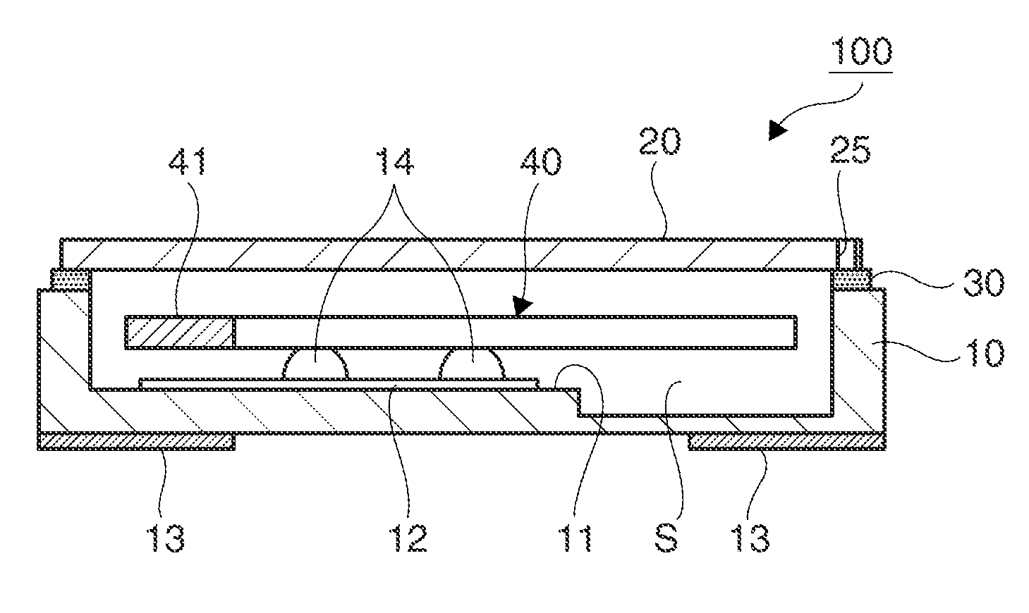
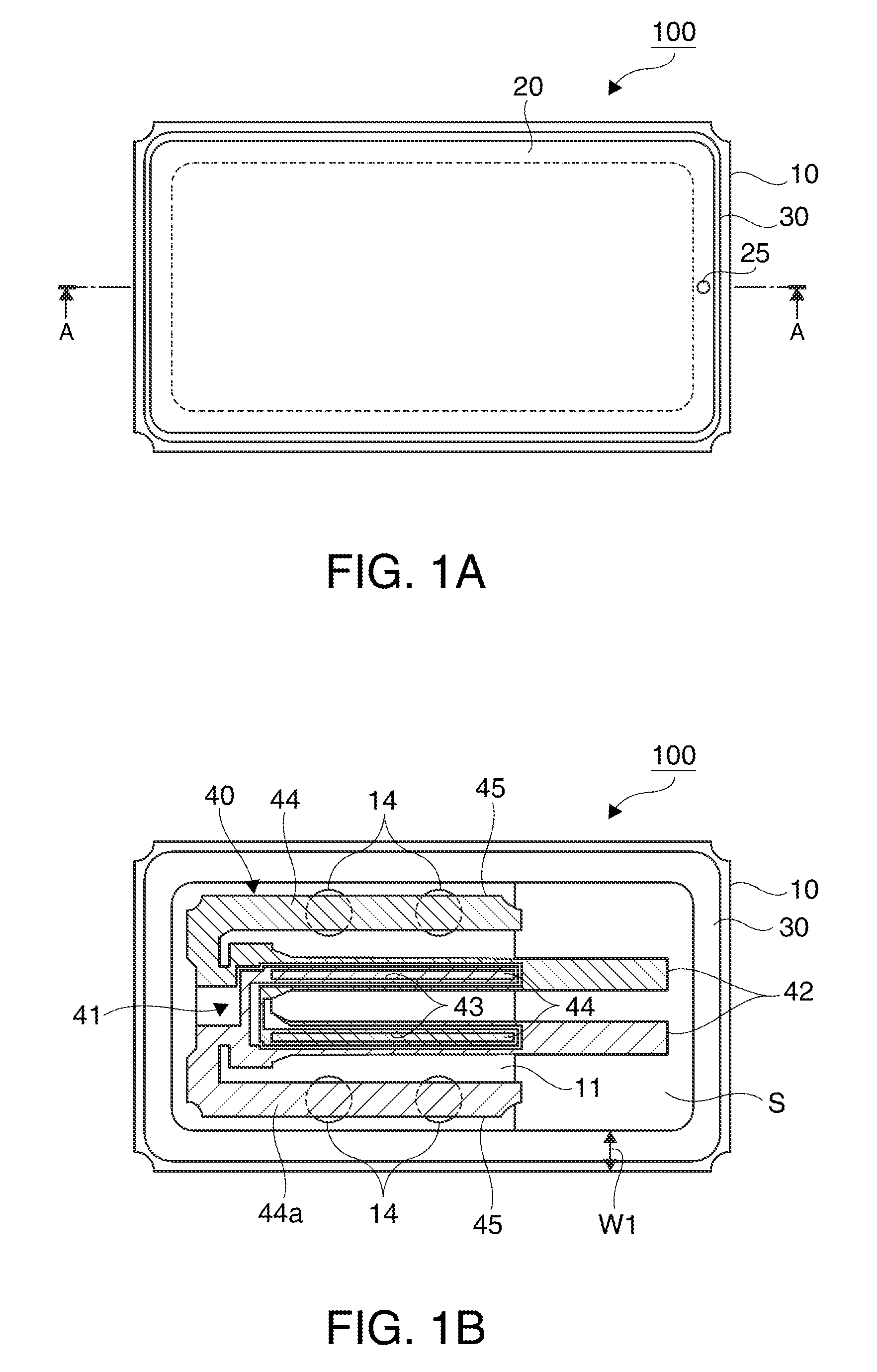
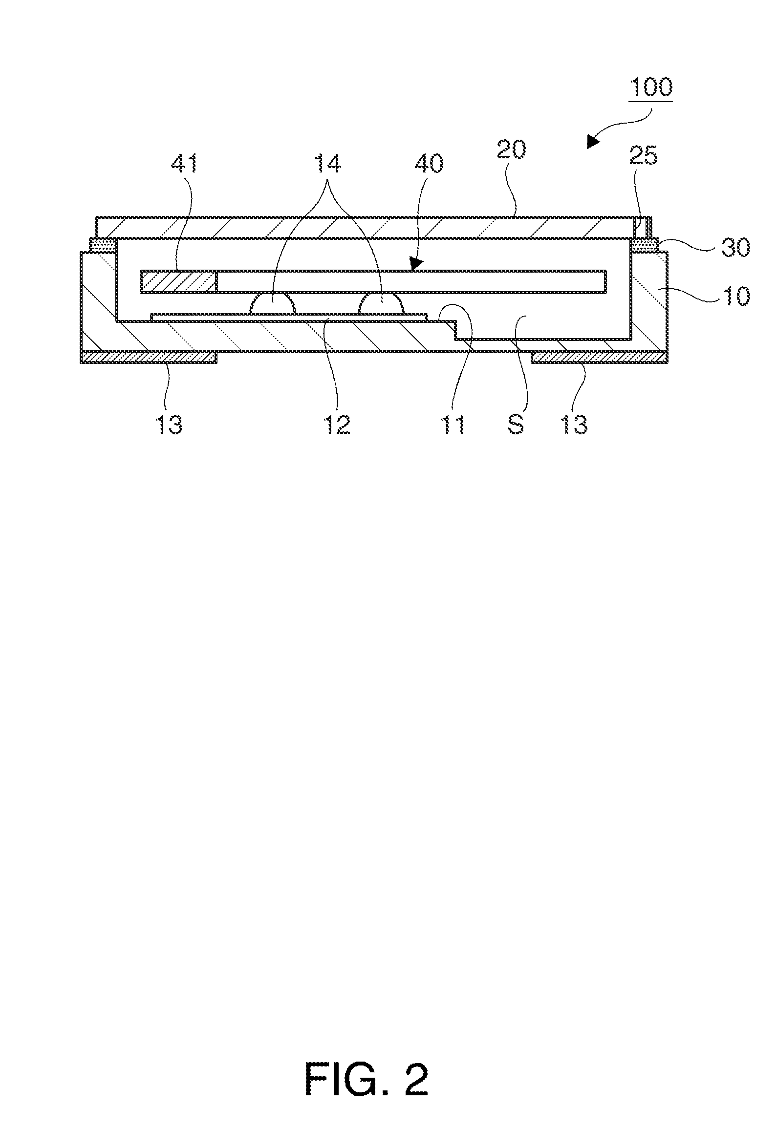
[0034]FIG. 1A is a plan view showing the appearance of an electronic device according to Embodiment 1 of the invention, and FIG. 1B is a plan view showing the inside of the electronic device in a state where a lid is removed. FIG. 2 is a sectional view showing the inside of the electronic device, and shows a section taken along the line A-A of the electronic device of FIG. 1A. As shown in the plan view of FIG. 1A, an electronic device 100 has a rectangular appearance in plan view, and includes a package 10, a lid 20, and a seam ring 30 which bonds the lid 20 to the package 10. In this case, the seam ring 30 is a metalization portion of the package 10, and the lid 20 has a seal hole (hole portion) 25 which is provided so as to overlap the seam ring 30 as a metalization portion in plan view. In this case, the seal hole 25 is provided at one place, and a circular through hole.
[0035]The package 10 of the electronic device 100 shown in FIG. 1B or 2 is molded using a ceramic green sheet m...
embodiment 2
[0052]Next, another preferred example of an electronic device manufactured by a method of manufacturing an electronic device will be described. FIG. 5 is a sectional view showing the bonded configuration of a package, a lid, and a seal hole of an electronic device according to Embodiment 2. An electronic device 200 has the same configuration as the electronic device 100, except that only the bonded configuration of the package 10, the lid 20, and the seal hole 25a is different from the electronic device 100 of Embodiment 1. In the electronic device 200, the seam ring 30 is bonded to the package 10, and a silver (Ag) solder 28 is arranged on the entire lid surface 20a of the lid 20 as the surface side placed to face the seam ring 30.
[0053]The lid 20 is placed on the seam ring 30, and if bonding is made by seam-welding and energy beam irradiation, the bonded state shown in FIG. 5 is made. The outer circumferential portion 20b of the lid 20 has a similar shape smaller than the outer ci...
embodiment 3
[0056]Next, another preferred example of an electronic device manufactured by a method of manufacturing an electronic device will be described. FIG. 6A is a plan view showing the configuration of an electronic device according to Embodiment 3, and FIG. 6B is a sectional view showing the bonded configuration of a package, a lid, and a seal hole. FIG. 6A shows a crystal vibrating piece 40 which is accommodated in the internal space S in a state where the lid 20 is removed. An electronic device 300 has the same configuration as the electronic device 100 or 200, except that the shape in plan view of the internal space S and the bonded configuration of the package 10, the lid 20, and the seal hole 25 are different from the electronic device 100 of Embodiment 1 or the electronic device 200 of Embodiment 2.
[0057]As shown in FIG. 6A, in the electronic device 300, the internal space S of the package 10 is narrowed inwardly at one corner of a rectangular shape. That is, the surface of the pac...
PUM
| Property | Measurement | Unit |
|---|---|---|
| temperature | aaaaa | aaaaa |
| melting point | aaaaa | aaaaa |
| melting point | aaaaa | aaaaa |
Abstract
Description
Claims
Application Information