Lighting apparatus

a technology of light source and light source, which is applied in the direction of lighting and heating apparatus, lighting support devices, fixed installations, etc., can solve the problems of significantly low efficiency of natural convection transmission to the surrounding atmosphere, and achieve the effects of improving light output, reducing heat radiation efficiency, and increasing the lifespan of light sources

Inactive Publication Date: 2014-02-13
SAMSUNG ELECTRONICS CO LTD
View PDF8 Cites 53 Cited by
  • Summary
  • Abstract
  • Description
  • Claims
  • Application Information

AI Technical Summary

Benefits of technology

[0006]An aspect of an exemplary embodiment provides a lighting apparatus, that may be capable of increasing a lifespan of a light source and improvin

Problems solved by technology

Such a heat transfer to the surrounding atmosphere through natural convection exhibits a significantly

Method used


Image

  • Lighting apparatus
  • Lighting apparatus
  • Lighting apparatus

Examples


first example

[0194]FIG. 32 is a side sectional view schematically illustrating an example of a light emitting device as a light emitting diode (LED) chip.

[0195]As illustrated in FIG. 32, a light emitting device 2000 may include a light emitting laminate L formed on a substrate 2001. The light emitting laminate L may include a first conductivity-type semiconductor layer 2004, an active layer 2005, and a second conductivity-type semiconductor layer 2006.

[0196]Also, an ohmic-contact layer 2008 may be formed on the second conductivity-type semiconductor layer 2006, and first and second electrodes 2009a and 2009b may be formed on upper surfaces of the first conductivity-type semiconductor layer 2004 and the ohmic-contact layer 2008, respectively.

[0197]In the present disclosure, terms such as ‘upper portion’, ‘upper surface’, ‘lower portion’, ‘lower surface’, ‘lateral surface’, and the like, are determined based on the drawings, and in actuality, the terms may be changed according to a direction in wh...

second example

[0229]In the case of manufacturing a large light emitting device for high output, an LED chip illustrated in FIG. 33 promoting current spreading efficiency and heat dissipation efficiency may be provided.

[0230]As illustrated in FIG. 33, an LED chip 2100 may include a first conductivity-type semiconductor layer 2104, an active layer 2105, a second conductivity-type semiconductor layer 2106, a second electrode layer 2107, an insulating layer 2102, a first electrode layer 2108 and a substrate 2101 sequentially laminated. Here, in order to be electrically connected to the first conductivity-type semiconductor layer 2104, the first electrode layer 2108 includes one or more contact holes H extending from one surface of the first electrode layer 2108 to at least a partial region of the first conductivity-type semiconductor layer 2104 and electrically insulated from the second conductivity-type semiconductor layer 2106 and the active layer 2105. However, the first electrode layer 2108 is no...

third example

[0240]An LED lighting device provides improved heat dissipation characteristics, and in terms of overall heat dissipation performance, an LED chip having a low heating value is preferably used in a lighting device. As an LED chip satisfying such requirements, an LED chip including a nano-structure therein (hereinafter, referred to as a ‘nano-LED chip’) may be used.

[0241]Such a nano-LED chip includes a recently developed core / shell type nano-LED chip, which has a low binding density to generate a relatively low degree of heat, and has increased luminous efficiency by increasing a light emitting area by utilizing nano-structures, prevents a degradation of efficiency due to polarization by obtaining a non-polar active layer, thus improving drop characteristics such that luminous efficiency is reduced as an amount of injected current is increased.

[0242]FIG. 34 illustrates a nano-LED chip as another example of an LED chip that may be employed in the foregoing lighting device.

[0243]As ill...


PUM

PropertyMeasurementUnit
Sizeaaaaaaaaaa
Shapeaaaaaaaaaa
Radiusaaaaaaaaaa

Abstract

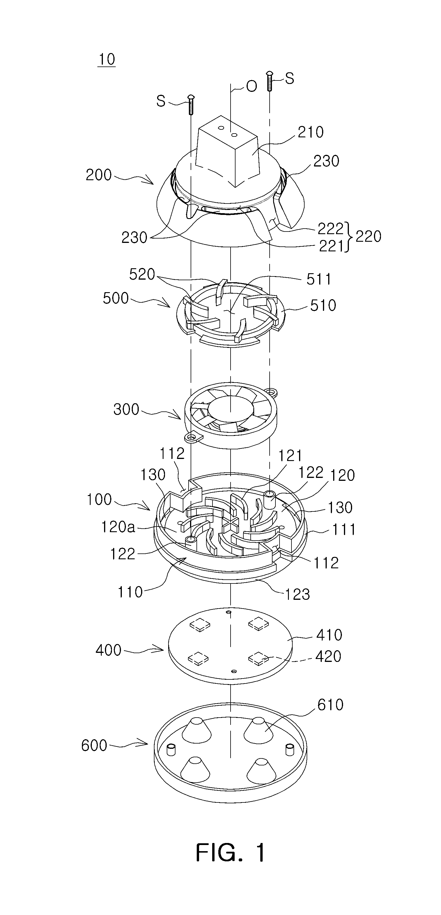
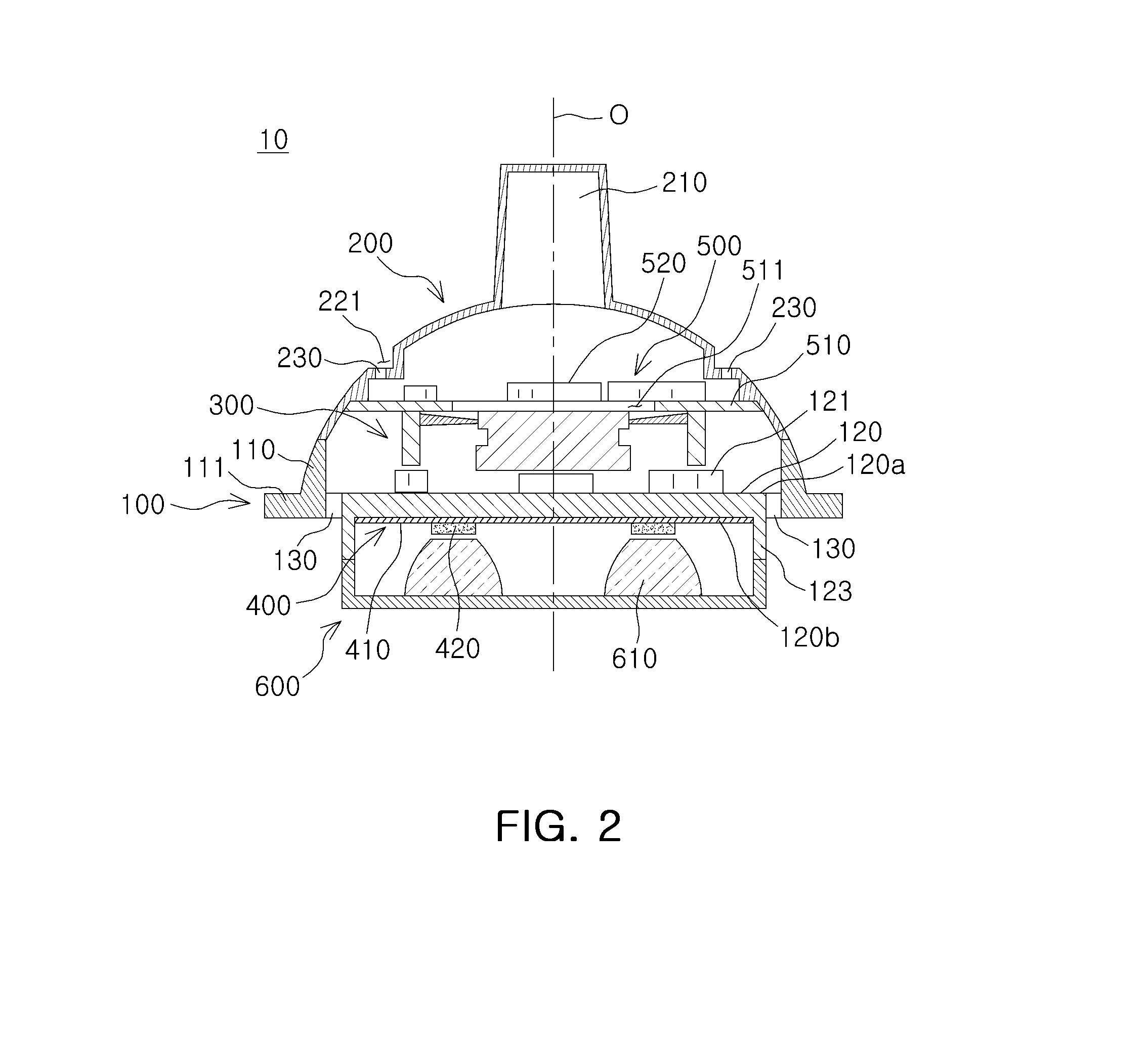
A lighting apparatus including a base with a coupling rim and a supporting plate and a housing coupled to the coupling rim such that the supporting plate is covered. The housing includes a channel part to guide air in and an air introduction hole to introduce the guided air into an inner space of the housing. A cooling fan is included and is disposed on an upper surface of the supporting plate covered by the housing, wherein the cooling fan draws air introduced through the air introduction hole into the inner space of the housing, and discharges the in-drawn air outside through an air discharging hole in the base. A light source module is included and mounted on a lower surface of the supporting plate, wherein the channel part provides a region depressed in a stepped manner along an outer surface of the housing.

Description

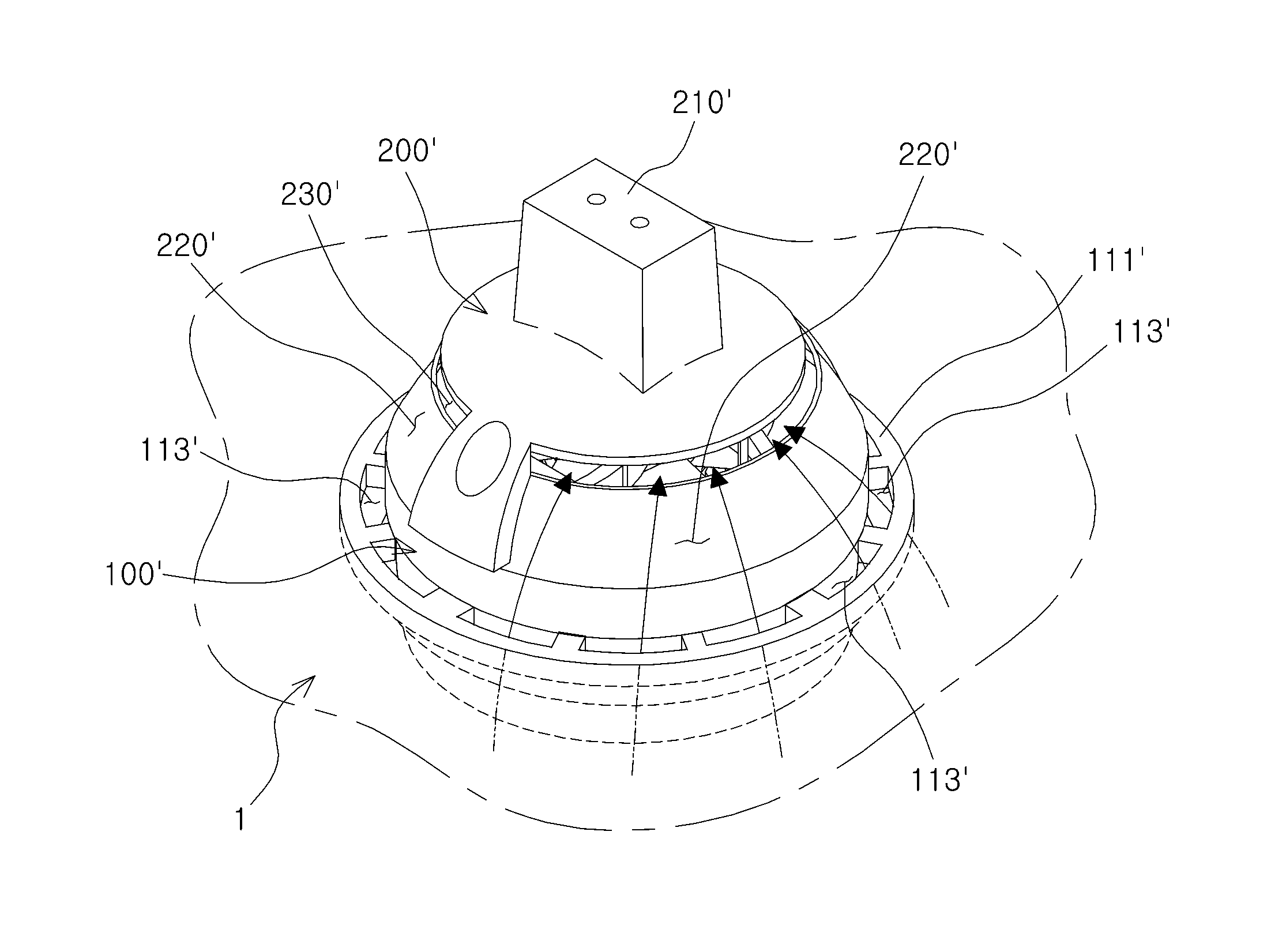
CROSS-REFERENCE TO RELATED APPLICATIONS[0001]This application claims the priority from Korean Patent Application No. 10-2012-0087933 filed in the Korean Intellectual Property Office on Aug. 10, 2012, and Korean Patent Application No. 10-2013-0073701 filed on Jun. 26, 2013, in the Korean Intellectual Property Office, the disclosures of which are incorporated herein by reference in there entireties.BACKGROUND[0002]1. Field[0003]Apparatuses and methods consistent with exemplary embodiments relate to a lighting apparatus, more particularly, to a lighting apparatus including a base, a housing, a cooling fan, and a lighting source.[0004]2. Description of the Related Art[0005]A lighting apparatus using a light emitting diode (LED) as a light source may transfer heat generated from the light source through a substrate to a heat sink and emit the heat into the surrounding atmosphere. Such a heat transfer to the surrounding atmosphere through natural convection exhibits a significantly low ef...

Claims


Application Information

Patent Timeline
IPC IPC(8): F21V29/02F21V5/04F21V15/01F21V29/00F21V13/04
CPCF21V29/025F21V29/2206F21V5/04F21V15/011F21V13/04F21S8/026F21V29/506F21V29/507F21V29/677F21V29/74F21V29/83F21Y2115/10F21V3/061F21V3/062F21V5/10H01L2224/48091H01L2924/181H05K1/053H05K1/056H05K3/107H05K2201/09154H05K2201/09845H05K2201/10106H05B47/19H05B47/195H01L2924/00014H01L2924/00012
Inventor JO, SOK HYUNYOON, SANG HOLEE, WOOK PYOKIM, HYUNG JIN
Owner SAMSUNG ELECTRONICS CO LTD
Why Eureka
Try Eureka