Multi-cavity wiring board for semiconductor assembly with internal electromagnetic shielding

a technology of electromagnetic shielding and wiring board, which is applied in the direction of printed circuit aspects, cross-talk/noise/interference reduction, and semiconductor/solid-state device details, etc., can solve the problems of increasing serious undesirable interference, unable to offer proper emi shielding or effective electromagnetic protection at the wiring board level, and unable to meet the requirements of the application

Inactive Publication Date: 2014-02-20
BRIDGE SEMICON
View PDF3 Cites 50 Cited by
  • Summary
  • Abstract
  • Description
  • Claims
  • Application Information

AI Technical Summary

Benefits of technology

[0017]The present invention also provides a semiconductor assembly in which semiconductor devices such as chips extend within the apertures of the stiffener and are electrically connected to the coreless substrate. Specifically, the semiconductor device can be flip mounted on the coreless substrate or the interposer within the aperture by solder bumps on the electrical pads of the coreless substrate or the second contact pads of the interposer. Alternatively, the semiconductor device may be mounted on the thermal paddle and electrically connected to the electrical pads by wire bonds. Accordingly, the signal contact pads of the semiconductor device can be electrically connected to the signal transduction pathways of the wiring board by signal electrical pads. The ground contact pads of the semiconductor device can be electrically connected to the lateral shielding sidewalls of the stiffener by ground electrical pads. Further, the semiconductor devices located within different apertures of the stiffener can be completely enclosed by the lateral shielding sidewalls of the stiffener in the lateral directions and be spaced from one another by the stiffener. As a result, each semiconductor device can be shielded from electromagnetic interference signals from others by the metal layer of the aperture sidewalls that completely covers peripheral edges of the semiconductor device in the lateral directions.

Problems solved by technology

The semiconductor devices are susceptible to electromagnetic interference (EMI) or other inter-device interference, such as capacitive, inductive, conductive coupling when operated in a high frequency mode.
These undesirable interferences may become increasingly serious when the semiconductor dies are placed closely together for the miniaturization purpose.
None of these approaches offers a proper EMI shielding or effective electromagnetic protection at the wiring board level especially when the semiconductor dies are disposed side-by-side on a board.

Method used


Image

  • Multi-cavity wiring board for semiconductor assembly with internal electromagnetic shielding
  • Multi-cavity wiring board for semiconductor assembly with internal electromagnetic shielding
  • Multi-cavity wiring board for semiconductor assembly with internal electromagnetic shielding

Examples


embodiment 1

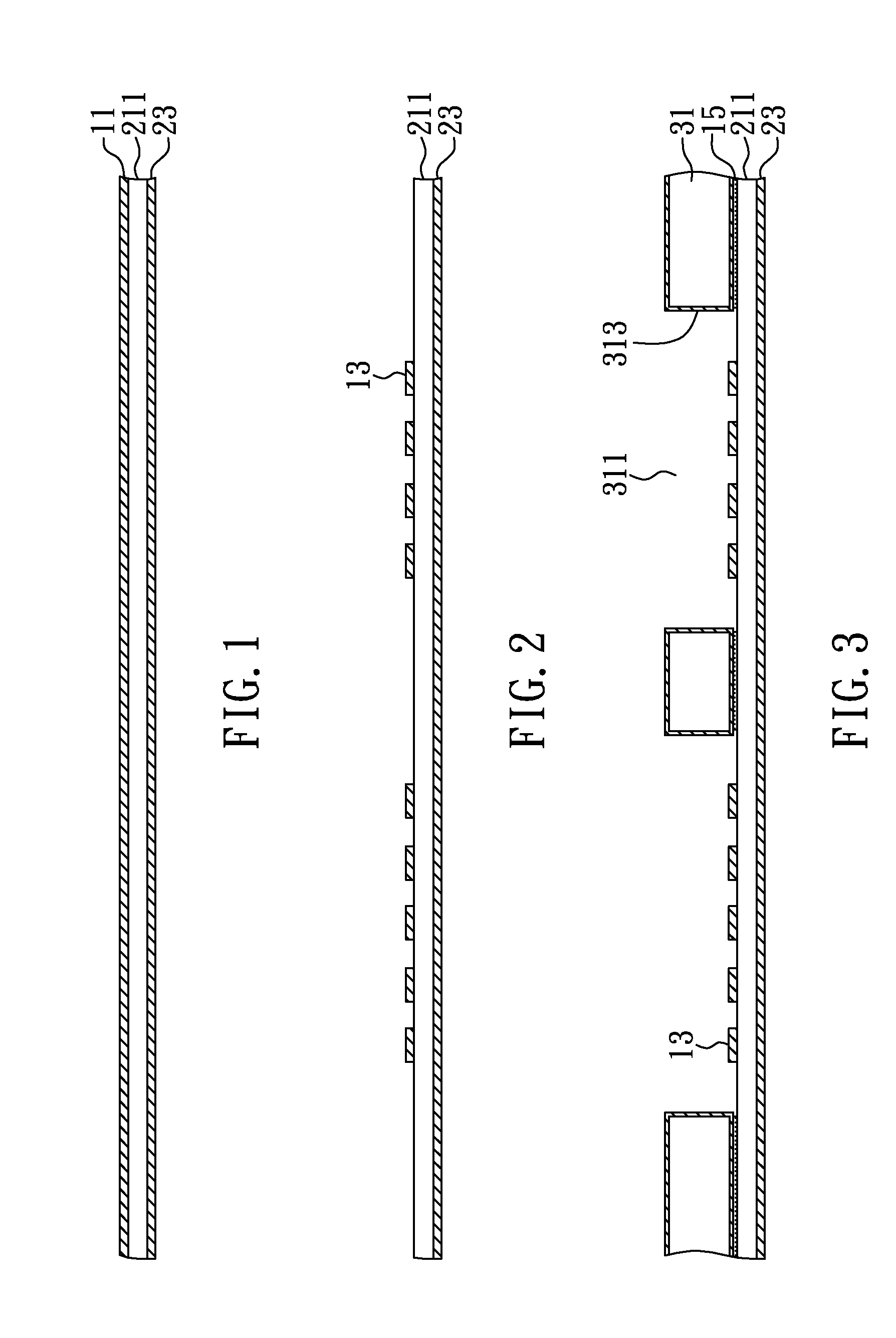
[0027]FIGS. 1-8 are cross-section views showing a method of making a multi-cavity wiring board that includes a careless substrate, an adhesive, and a stiffener having multiple apertures with lateral shielding sidewalls in accordance with an embodiment of the present invention.

[0028]As shown in FIG. 8, multi-cavity wiring board 100 includes stiffener 31, adhesive 15 and coreless substrate 201. Stiffener 31 includes multiple apertures 311 with lateral shielding sidewalls and is affixed on coreless substrate 201 using adhesive 15. In this illustration, coreless substrate 201 includes electrical pads 13, first dielectric layer 211, first conductive traces 231, second dielectric layer 251 and second conductive traces 271. First conductive traces 231 are electrically connected to electrical pads 13 for signal routing, and also provide an electrical interconnection between electrical pads 13 and stiffener 31 for grounding the lateral shielding sidewalls of apertures 311.

[0029]FIG. 1 is a c...

embodiment 2

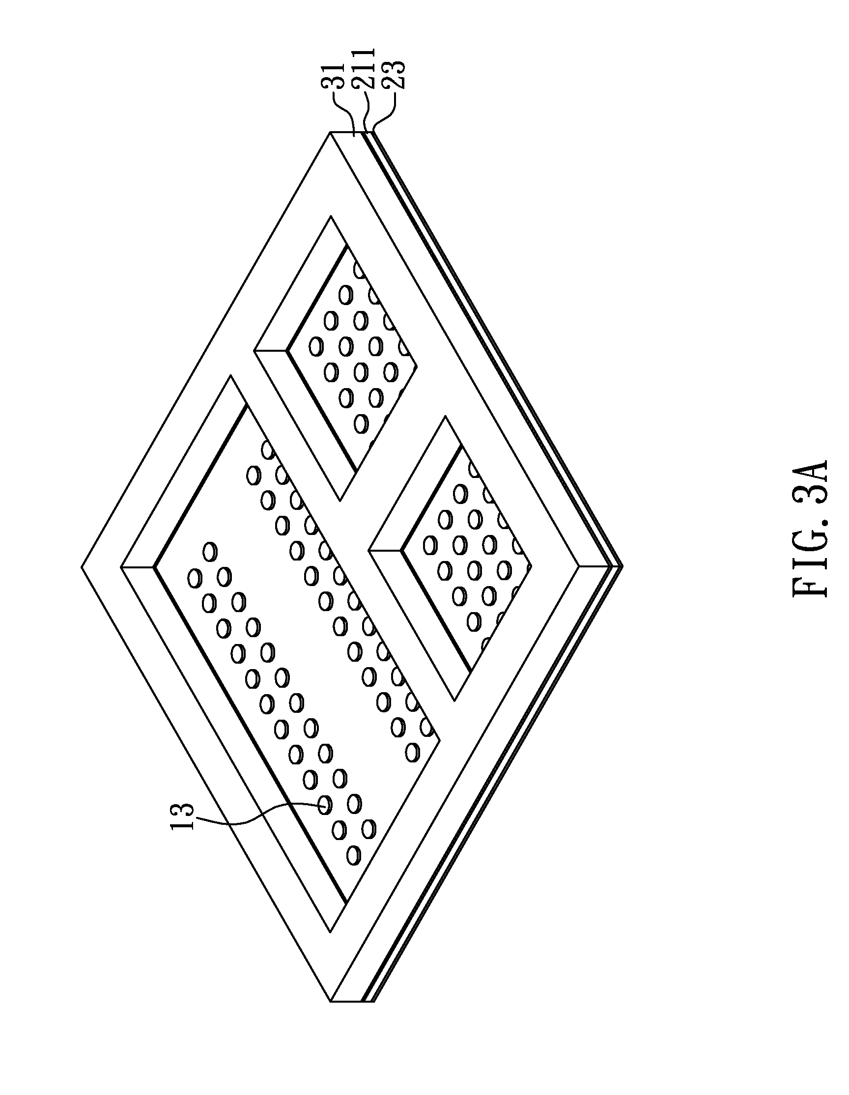
[0044]FIGS. 11 and 11A are cross-sectional and top views, respectively, of another multi-cavity wiring board 200 with plated through holes 411 as electrical connection between metallic sidewalls of apertures 311 and electrical pads 13 in accordance with another embodiment of the present invention.

[0045]In this embodiment, multi-cavity wiring board 200 is manufactured in a manner similar to that illustrated in Embodiment 1, except that the metallic sidewalls of apertures 311 are electrically connected to electrical pads 13 by first conductive traces 231 and plated through holes 411 that extend from conductive layer 313 on the top surface of stiffener 31 to first conductive traces 231 through stiffener 31, adhesive 15 and first dielectric layer 211 in vertical directions. Plated through holes 411 are formed by forming through holes 401 after attaching stiffener 31 and then depositing connecting layer 402 on the sidewall of through holes 401 during depositing first conductive traces 23...

embodiment 3

[0047]FIGS. 12-18 are cross-section views showing a method of making yet another multi-cavity wiring board with electrical pads, thermal paddles, stoppers and placement guide exposed from metallic apertures of a stiffener in accordance with yet another embodiment of the present invention.

[0048]For purposes of brevity, any description in above Embodiments is incorporated herein insofar as the same is applicable, and the same description need not be repeated.

[0049]FIGS. 12 and 12A are cross-sectional and top views, respectively, of the structure with stoppers 16 formed on metal layer 11 of laminate substrate. As illustrated in above embodiments, the laminate substrate includes metal layer 11, first dielectric layer 211 and support plate 23. Stoppers 16 can be formed by electrolytic plating of metal on metal layer 11 using photolithographic process. In this illustration, each stopper 16 consists of plural metal posts in a rectangular frame array with a thickness of 35 microns and confo...


PUM


Abstract

A multi-cavity wiring board includes a coreless substrate, an adhesive, and a stiffener having a plurality of apertures with lateral shielding sidewalls. The coreless substrate covers the stiffener and includes electrical pads exposed from the apertures of the stiffener as electrical contacts for semiconductor devices packaged within the apertures. The aperture sidewalls of the stiffener can serve as effective lateral electromagnetic shields for the semiconductor devices within the apertures.

Description

CROSS REFERENCE TO RELATED APPLICATION[0001]This application is a continuation-in-part of U.S. application Ser. No. 13 / 615,819 filed Sep. 14, 2012, a continuation-in-part of U.S. application Ser. No. 13 / 753,625 filed Jan. 30, 2013 and a continuation-in-part of U.S. application Ser. No. 13 / 733,226 filed Jan. 3, 2013, each of which is incorporated by reference. This application also claims the benefit of filing date of U.S. Provisional Application Ser. No. 61 / 731,564 filed Nov. 30, 2012.[0002]U.S. application Ser. No. 13 / 753,625 filed Jan. 30, 2013 is a continuation-in-part of U.S. application Ser. No. 13 / 615,819 filed Sep. 14, 2012. U.S. application Ser. No. 13 / 615,819 filed Sep. 14, 2012, U.S. application Ser. No. 13 / 753,625 filed Jan. 30, 2013 and U.S. application Ser. No. 13 / 733,226 filed Jan. 3, 2013 all claim the benefit of filing date of U.S. Provisional Application Ser. No. 61 / 682,801 filed Aug. 14, 2012.BACKGROUND OF THE INVENTION[0003]1. Field of the Invention[0004]The prese...

Claims


Application Information

Patent Timeline
Patent Type & Authority Applications(United States)
IPC IPC(8): H05K9/00
CPCH05K9/00H01L2224/16145H01L2224/16225H01L2224/32225H01L2224/32245H01L2224/48091H01L2224/48227H01L2224/73204H01L2224/73253H01L2224/73265H01L2924/15192H01L2924/15311H01L2924/3025H05K1/0216H05K1/186H05K2201/09781H05K2201/10515H05K2201/10553H05K2201/10674H05K1/0206H05K3/284H05K3/4697H05K2201/0715H05K2201/10969H01L23/552H01L25/16H01L24/73H01L2224/26175H01L2224/8314H01L2924/3511H01L2924/00012H01L2924/00H01L2924/00014
Inventor LIN, CHARLES W.C.WANG, CHIA-CHUNG
Owner BRIDGE SEMICON
Why Eureka
Try Eureka