Techniques for Metal Gate Work Function Engineering to Enable Multiple Threshold Voltage Nanowire FET Devices

a technology of nanowires and function engineering, applied in the field of gate work function engineering, can solve the problems of multiple threshold voltage (vt) devices, becomes extremely problematic, and requires a substantial amount of process complexity

US20140048773A1Active Publication Date: 2014-02-20GLOBALFOUNDRIES US INC
3 Cites 19 Cited by

Patent Information

Authority / Receiving Office
US · United States
Patent Type
Applications(United States)
Current Assignee / Owner
Publication Date
2014-02-20

Smart Images

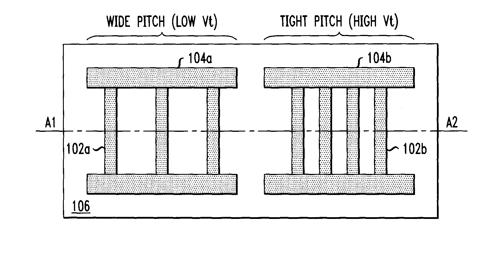
  • Figure 1
    Figure 1
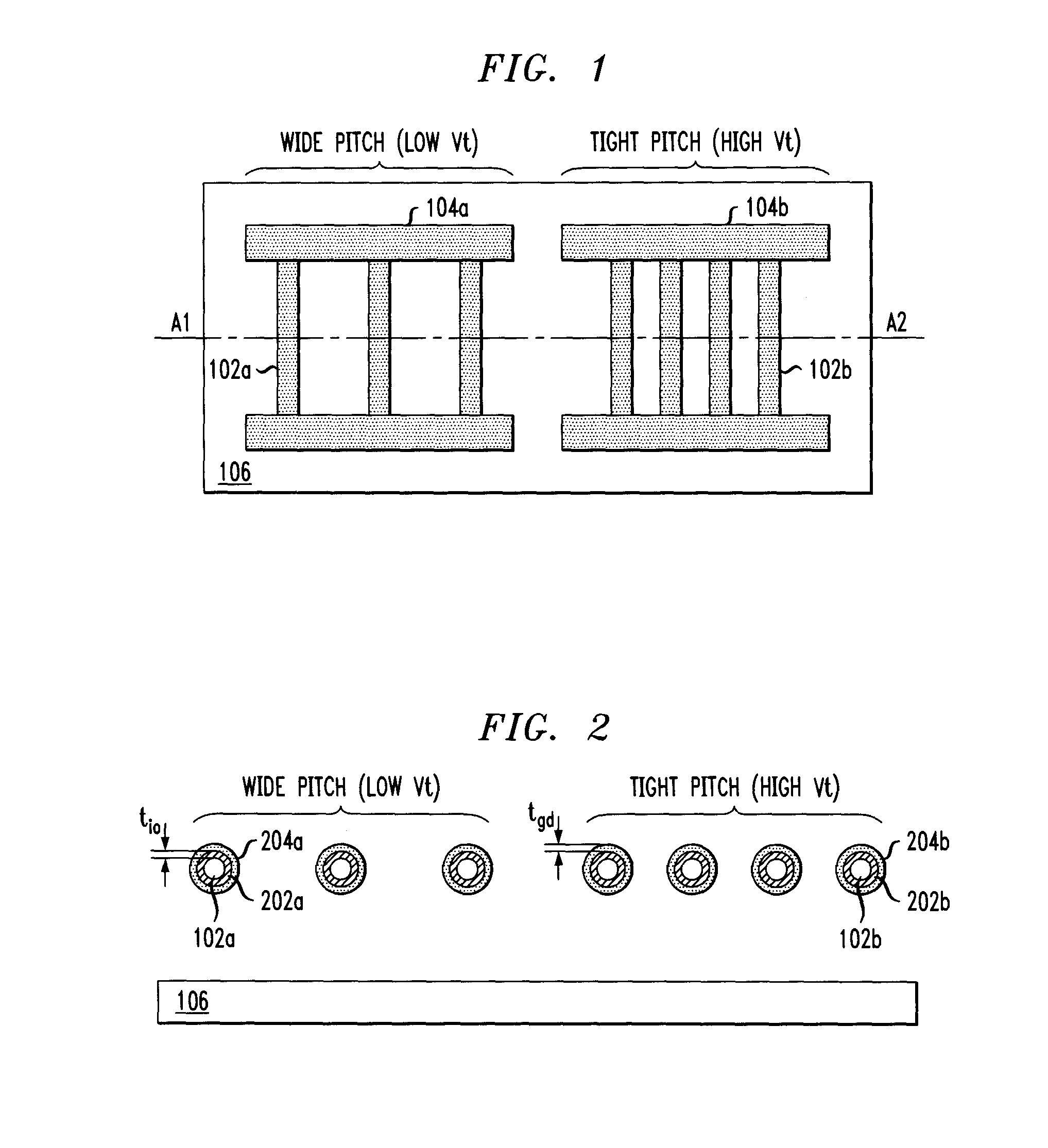
  • Figure 2
    Figure 2
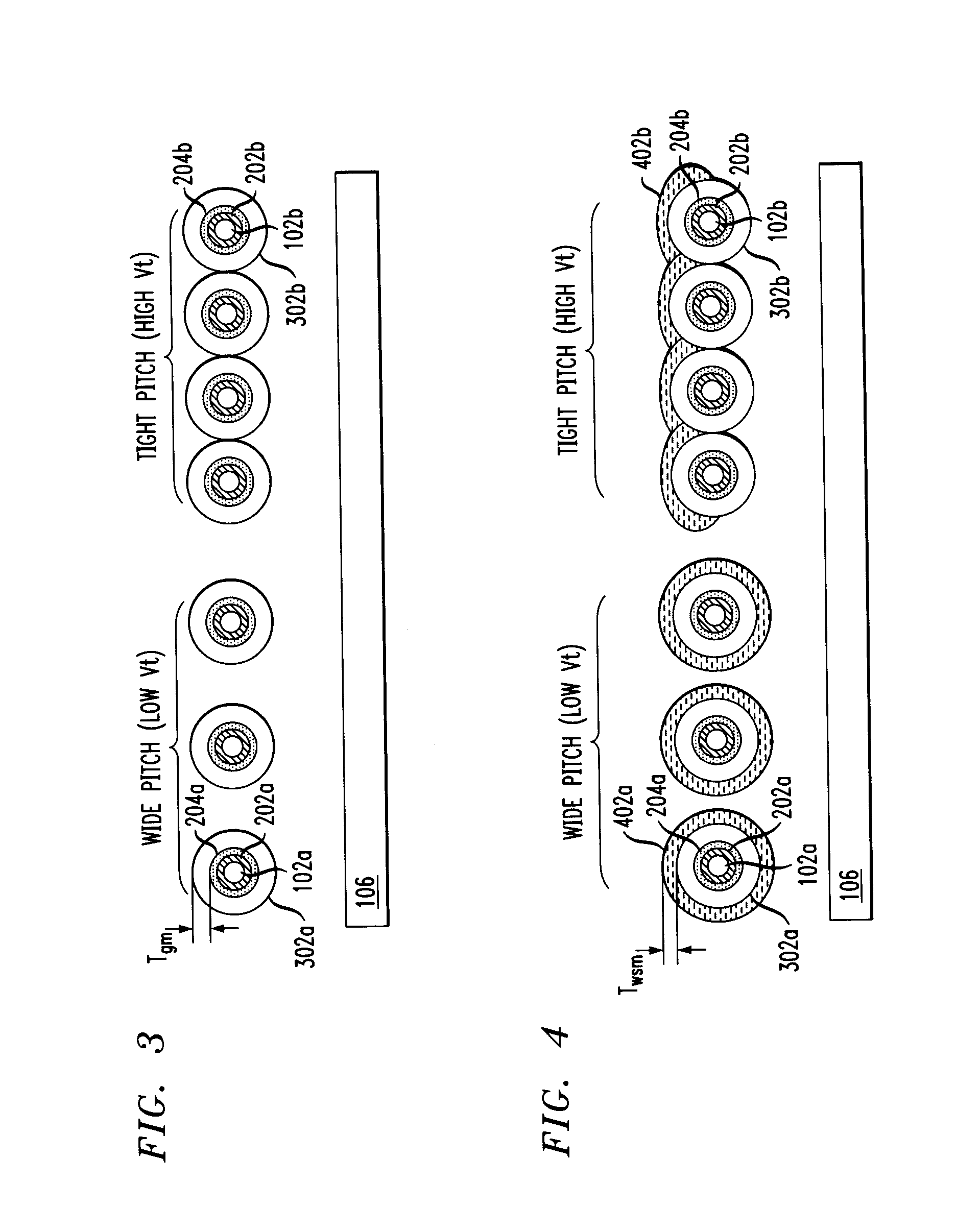
  • Figure 3
    Figure 3
Patent Text Reader

Abstract

A nanowire FET device includes a SOI wafer having a SOI layer over a BOX, and a plurality of nanowires and pads patterned in the SOI layer, wherein the nanowires are suspended over the BOX; an interfacial oxide surrounding each of the nanowires; and at least one gate stack surrounding each of the nanowires, the gate stack having (i) a conformal gate dielectric present on the interfacial oxide (ii) a conformal first gate material on the conformal gate dielectric (iii) a work function setting material on the conformal first gate material, and (iv) a second gate material on the work function setting material. A volume of the conformal first gate material and / or a volume of the work function setting material in the gate stack are / is proportional to a pitch of the nanowires.
Need to check novelty before this filing date? Find Prior Art

Description

CROSS-REFERENCE TO RELATED APPLICATION(S)

[0001] This application is a continuation of U.S. application Ser. No. 13 / 588,724 filed on Aug. 17, 2012, the disclosure of which is incorporated by reference herein.FIELD OF THE INVENTION

[0002] The present invention relates to nanowire field-effect transistor (FET) devices, and more particularly, to techniques for gate work function engineering using a work function setting material an amount of which is provided proportional to nanowire pitch so as to enable multiple threshold voltage (Vt) devices.BACKGROUND OF THE INVENTION

[0003] In current complementary metal-oxide semiconductor (CMOS) scaling, the use of undoped gate all around (GAA) nanowire devices is a highly investigated structure as a device choice for future CMOS. One key problem with undoped devices is the implementation of multiple threshold voltage (Vt) devices. One solution is to dope the nanowire FET. To do so, however, for aggressively scaled devices has serious drawbacks from r...

Examples

Embodiment Construction

[0018]As described above, there are notable disadvantages associated with using doping and / or different work function gate stacks to produce multiple threshold voltage (Vt) nanowire field-effect transistor (FET) devices. Advantageously, provided herein are techniques for producing multiple Vt nanowire FET devices using a work function setting material in an amount that is modulated as a function of nanowire pitch (wire to wire pitch, where the pitch is defined as the distance from the center of one nanowire to the adjacent nanowire(s)). Namely, a thickness of the materials in the device gate stacks will be chosen such that less work function setting material ends up in the tighter pitch nanowire FETs. Thus, for smaller pitch, higher nanowire FET Vt is obtained and therefore, through nanowire pitch variation, different Vt devices may be fabricated. The technique does come at the cost of significant reduction in active width density, however if the lower Vt (wider pitch) devices are n...