Organic light-emitting device and method for manufacturing same

a light-emitting device and organic technology, applied in the direction of luminescent compositions, thermoelectric devices, chemistry apparatus and processes, etc., can solve the problems of difficult to manufacture an organic light-emitting device with high efficiency and a long life span, and difficult to apply npb to an organic light-emitting device requiring a high curren

Active Publication Date: 2014-02-20
LG CHEM LTD
View PDF5 Cites 94 Cited by
  • Summary
  • Abstract
  • Description
  • Claims
  • Application Information

AI Technical Summary

Benefits of technology

[0013]An organic light emitting device according to the present invention comprises a first electrode, a second electrode, and one or more organic material layers disposed between the first electrode and the second electrode, and a life-span property of the organic light emitting device can be largely improved by changing a dipole moment of a compound comprised in the organic material layers.

Problems solved by technology

Recently, since NPB, which has mainly been used as the hole transport layer material, has a glass transition temperature of 100° C. or lower, there is a problem in that it is difficult to apply NPB to an organic light emitting device requiring a high current.
In the case of PEDOT:PSS currently used as a hole transport material in an organic light emitting device manufactured by a solution coating method, since a LUMO energy level thereof is lower than that of an organic material used as a light emitting layer material, it is difficult to manufacture an organic light emitting device having high efficiency and a long life span.

Method used


Image

  • Organic light-emitting device and method for manufacturing same
  • Organic light-emitting device and method for manufacturing same
  • Organic light-emitting device and method for manufacturing same

Examples


experimental example 1

[0165]The life-span properties of the organic light emitting device where only the compound represented by Formula 12 is applied to the electron transport layer and the organic light emitting device where the compound represented by Formula 12 and the alkali metal complex (LiQ) are applied together to the electron transport layer were evaluated, and the result is described in the following FIG. 5. Herein, other constitution components of the organic light emitting device were the same, except that the compound constituting the electron transport layer was changed.

[0166]As shown in the following FIG. 5, it can be seen that the life-span property of the organic light emitting device of the present invention, in which the dipole moment of the compound comprised in the organic material layer is increased, is improved by two times as compared to the organic light emitting device in which the dipole moment thereof is not increased.

experimental example 2

[0167]The life-span properties of the organic light emitting device where only the compound represented by Formula 13 is applied to the electron transport layer and the organic light emitting device where the compound represented by Formula 13 and the alkali metal complex (LiQ) are applied together to the electron transport layer were evaluated, and the result is described in the following FIG. 6.

[0168]As shown in the following FIG. 6, it can be seen that the life-span property of the organic light emitting device of the present invention, in which the dipole moment of the compound comprised in the organic material layer is increased, is improved by four times as compared to the organic light emitting device in which the dipole moment thereof is not increased.

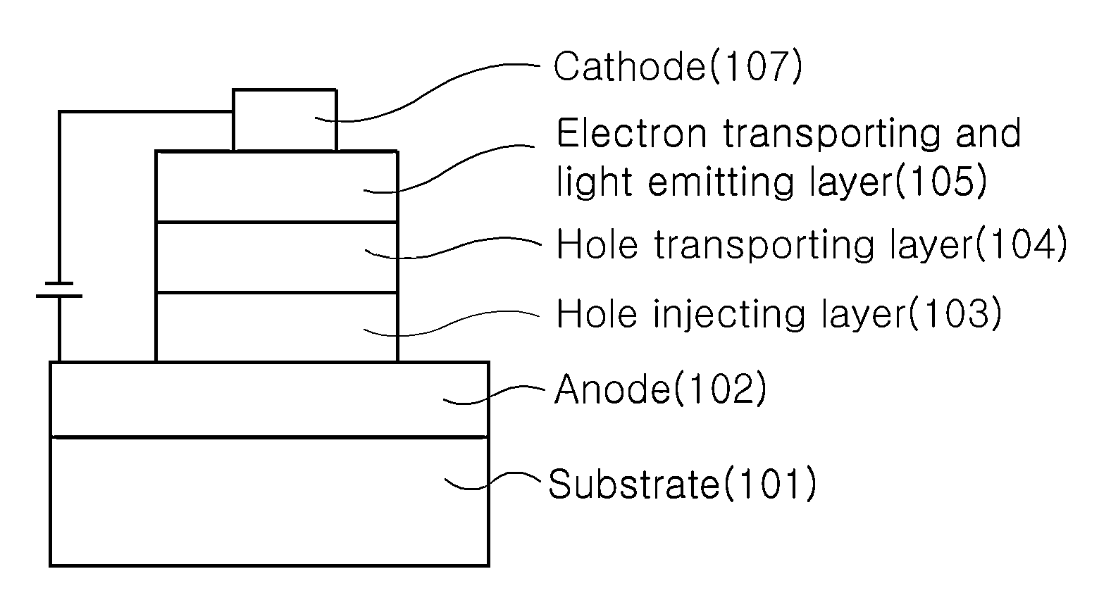
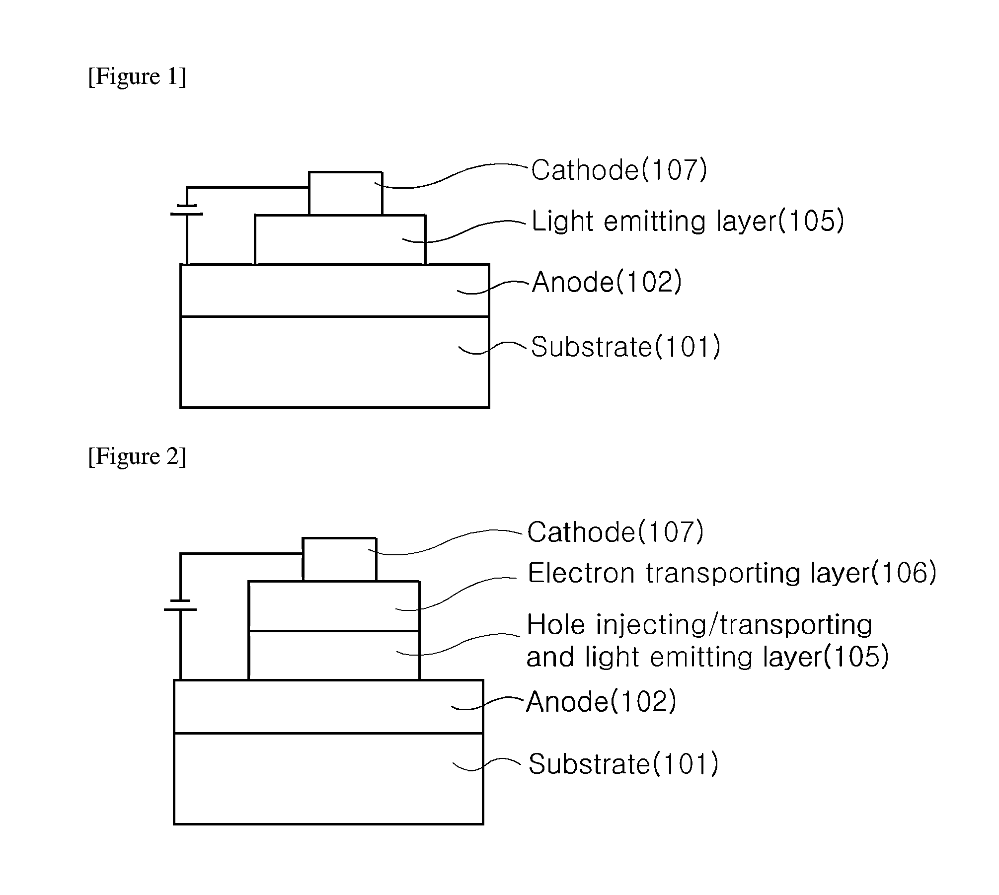
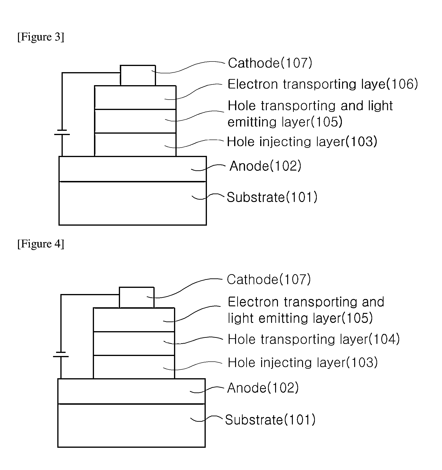
[0169]As described above, an organic light emitting device according to the present invention comprises a first electrode, a second electrode, and one or more organic material layers disposed between the first electrode and the...


PUM


Abstract

The present invention provides an organic light emitting device comprising a first electrode, a second electrode, and one or more organic material layers disposed between the first electrode and the second electrode, and having an excellent life-span property by changing a dipole moment of a compound comprised in the organic material layers.

Description

TECHNICAL FIELD[0001]This application claims priority from Korean Patent Application No. 10-2011-0101513 filed on Oct. 5, 2011, in the KIPO, the disclosure of which is incorporated herein by reference in its entirety.[0002]The present invention relates to an organic light emitting device and a method of manufacturing the same.BACKGROUND ART[0003]An organic light emitting phenomenon is an example of a conversion of current into visible rays by an internal process of a specific organic molecule. The organic light emitting phenomenon is based on the following principle. When an organic material layer is interposed between an anode and a cathode, if voltage is applied between two electrodes, electrons and holes are injected from the cathode and the anode to the organic material layer. The electrons and the holes injected into the organic material layer are recombined to form an exciton, and the exciton is reduced to a bottom state to emit light. The organic light emitting device using t...

Claims


Application Information

Patent Timeline
Patent Type & Authority Applications(United States)
IPC IPC(8): H01L51/00
CPCH01L51/0072H01L51/0071H01L51/0058H10K85/615H10K85/30H10K85/6572H10K50/00C09K11/06H10K85/626H10K85/657
Inventor CHUN, MINSEUNGJANG, JUNGISHIN, CHANGHWANKIM, SEONG SOLEE, HYUNGJINJEON, SANG YOUNGKIM, CHANG HWANKIM, DONG SIK
Owner LG CHEM LTD
Why Eureka
Try Eureka