Noise-resistant sampling circuit and image sensor

a sampling circuit and noise-resistant technology, applied in the field of sampling circuits, can solve the problems of not addressing the problems of related art, and the delicate image signal may be vulnerable to even a small amount of noise, so as to reduce the noise level of the voltage signal and reduce the noise in the signal

Inactive Publication Date: 2014-02-20
LUXEN TECH +1
View PDF2 Cites 14 Cited by
  • Summary
  • Abstract
  • Description
  • Claims
  • Application Information

AI Technical Summary

Benefits of technology

[0014]A third aspect of the present invention provides a method for reducing noise in a signal, comprising: amplifying a charge signal received from a photo diode with an amplifier to yield a voltage signal; passing the voltage signal from the amplifier through a low pass filter to reduce a noise level in the voltage signal; sampling and storing the voltage signal in a first sample and hold circuit; sampling and storing the voltage signal in a second sample and hold circuit; outputting the stored voltage signal from the first sample and hold circuit as a first reset signal; and outputting the stored voltage signal from the second sample and hold circuit as a second reset signal.

Problems solved by technology

These delicate image signals may be vulnerable to even a smallest amount of noise, necessitating reduction or elimination of noise factors (e.g., experienced during sampling and / or from external sources).
Unfortunately, none of these attempts address the issues of the related art.

Method used


Image

  • Noise-resistant sampling circuit and image sensor
  • Noise-resistant sampling circuit and image sensor
  • Noise-resistant sampling circuit and image sensor

Examples


Embodiment Construction

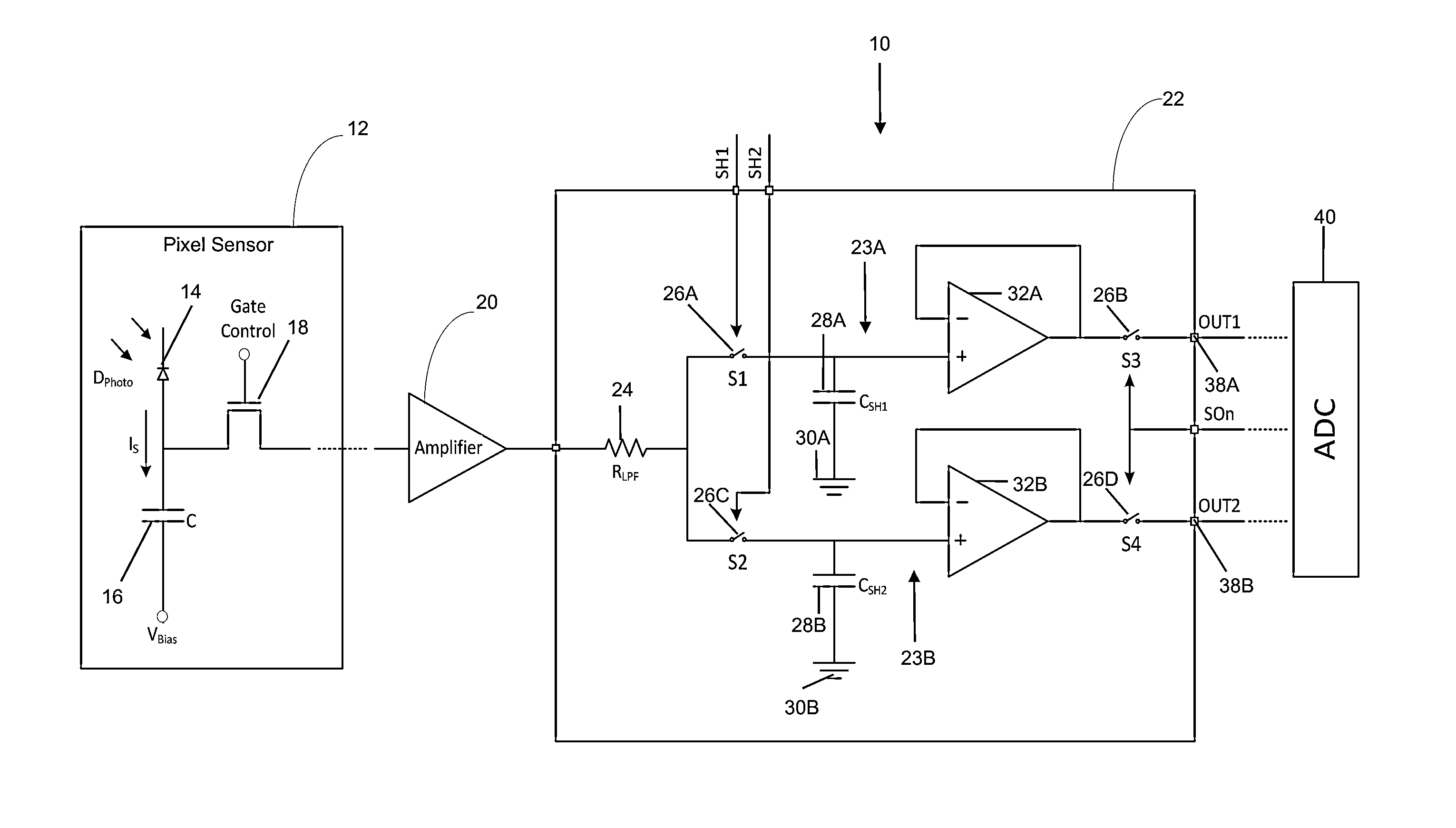
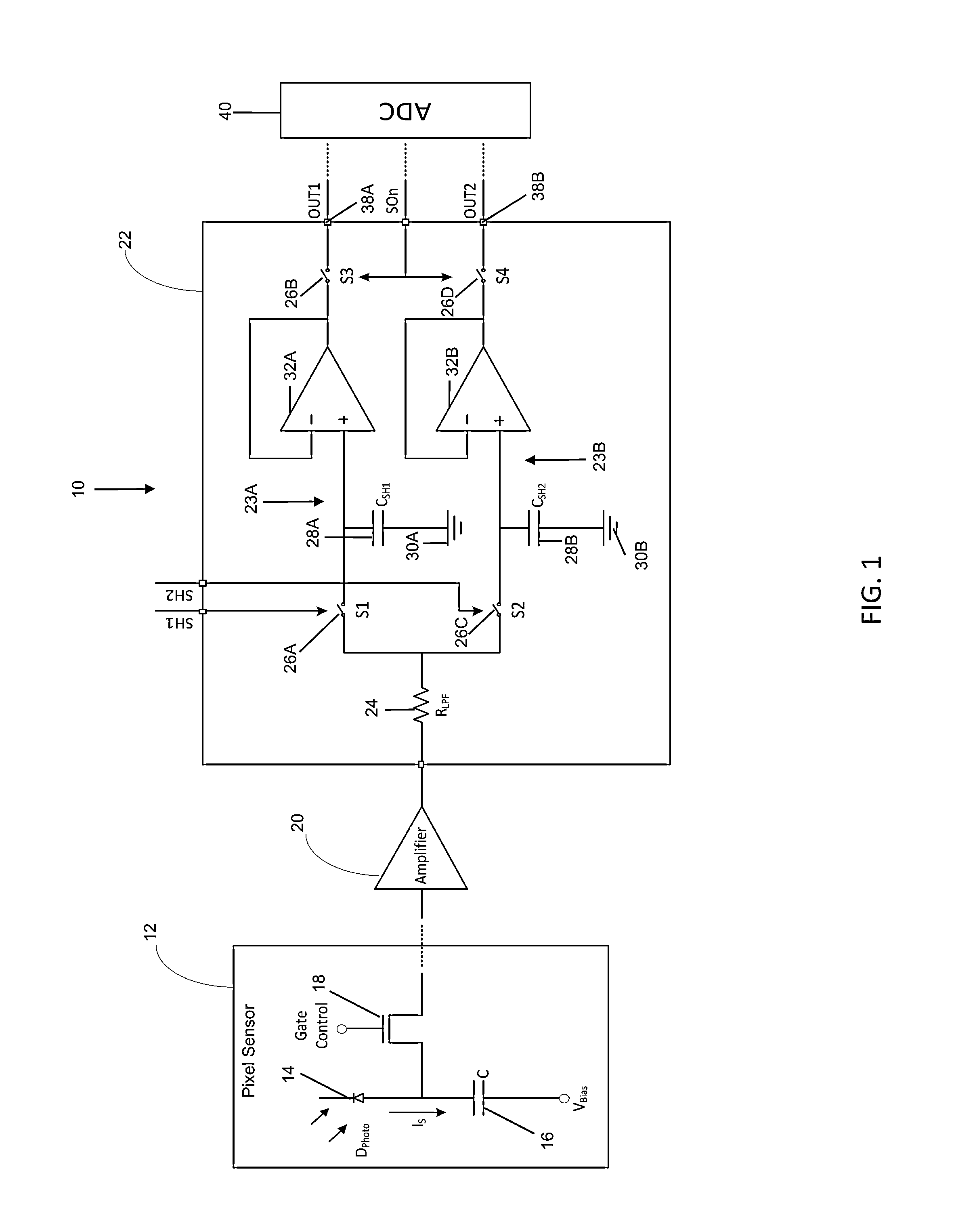
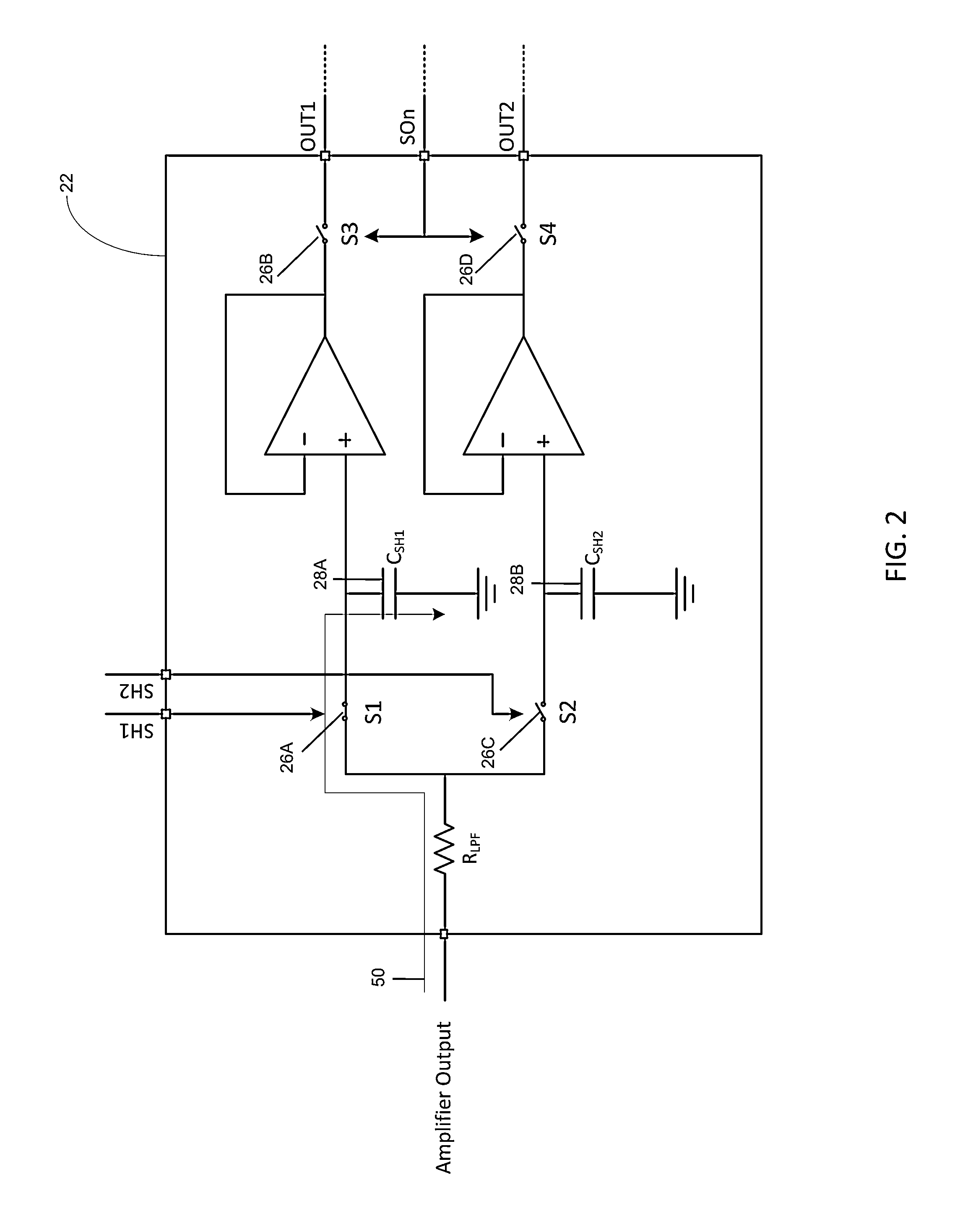
[0022]Illustrative embodiments will now be described more fully herein with reference to the accompanying drawings, in which exemplary embodiments are shown. This disclosure may, however, be embodied in many different forms and should not be construed as limited to the exemplary embodiments set forth herein. Rather, these exemplary embodiments are provided so that this disclosure will be thorough and complete and will fully convey the scope of this disclosure to those skilled in the art. In the description, details of well-known features and techniques may be omitted to avoid unnecessarily obscuring the presented embodiments.

[0023]The terminology used herein is for the purpose of describing particular embodiments only and is not intended to be limiting of this disclosure. As used herein, the singular forms “a”, “an”, and “the” are intended to include the plural forms as well, unless the context clearly indicates otherwise. Furthermore, the use of the terms “a”, “an”, etc., do not de...


PUM


Abstract

An approach for a sampling circuit to reduce noise in signals (e.g., as received from photo diodes or the like) is provided. In one embodiment of the present invention, there is a sampling circuit comprising: an amplifier, which amplifies charge signals generated at photo diodes and converts them to voltage signals; the first sample and hold circuit, which samples the voltage signal and charges the first capacitor according to the first switching signal, and outputs the stored charge as a reset signal based on a readout signal; the second sample and hold circuit, which samples the signals and charges the second capacitor according to the second switching signal that is non-overlapping to the first switching signal, and outputs the stored charge as a reset signal based on the readout signal; a resistor that acts as a low-pass filter placed in between the first and the second capacitors' common nodes.

Description

FIELD OF THE INVENTION[0001]In general, embodiments of the present invention relate to a sampling circuit. Specifically embodiments, of the present invention relate to a noise-resistant / reducing sampling circuit that amplifies charges created at photodiodes and coverts the amplified signals to voltage signals.BACKGROUND OF THE INVENTION[0002]Conventional image sensors adopt a two-dimensional arrayed structure of multiple pixels with photo diodes (photo sensor) attached on top of the pixel array. An amplifier from each pixel may receive charge signals generated at the photo diodes and convert the received charge signals into voltage signals. A correlated double sampling (CDS) circuit may extract image signals by comparing the voltage signals to a reset voltage. Extracted image signals may then be read out row by row.[0003]These delicate image signals may be vulnerable to even a smallest amount of noise, necessitating reduction or elimination of noise factors (e.g., experienced during...

Claims


Application Information

Patent Timeline
Patent Type & Authority Applications(United States)
IPC IPC(8): H03K5/00
CPCH03K5/00H04N25/616H04N25/60H04N25/75
Inventor SOH, MYUNG-JINSOH, SEUL-YI
Owner LUXEN TECH
Why Eureka
Try Eureka