Method for producing semiconductor device

a manufacturing method and semiconductor technology, applied in semiconductor devices, instruments, electrical devices, etc., can solve the problems of increasing the number of process steps and manufacturing costs, and achieve the effects of less photomasks, low manufacturing costs, and small number of process steps

Inactive Publication Date: 2014-02-20
SHARP KK
View PDF3 Cites 7 Cited by
  • Summary
  • Abstract
  • Description
  • Claims
  • Application Information

AI Technical Summary

Benefits of technology

[0033]According to the present invention, a resist layer used in forming gate electrodes (first resist layer and second resist layer) and a resist layer (thinned second resist layer) used in injecting an impurity into injection regions that differ between the second semiconductor layer of an LDD structure or offset structure TFT and the first semiconductor layer of a normal structure TFT are formed by using a single photomask. Therefore, it is possible to manufacture a semiconductor device having both LDD structure or offset structure TFTs and normal structure TFTs, with less photomasks, a smaller number of process steps, and low manufacturing cost. This makes it possible to minimize malfunction of the semiconductor device, and allow the semiconductor device to have an excellent function, while reducing the manufacturing cost.

Problems solved by technology

Such a manufacturing method had a problem in that it was necessary to add a photomask to form the resist layer that acts as a mask for the portions where the low-concentration impurity regions are to be formed, which caused an increase in the number of process steps and manufacturing cost.

Method used


Image

  • Method for producing semiconductor device
  • Method for producing semiconductor device
  • Method for producing semiconductor device

Examples


embodiment 1

[0066]In Embodiment 1, an active matrix driving liquid crystal display device S will be explained as an example of a display device having a semiconductor device of the present invention.

[0067]—Configuration of Liquid Crystal Display Device S—

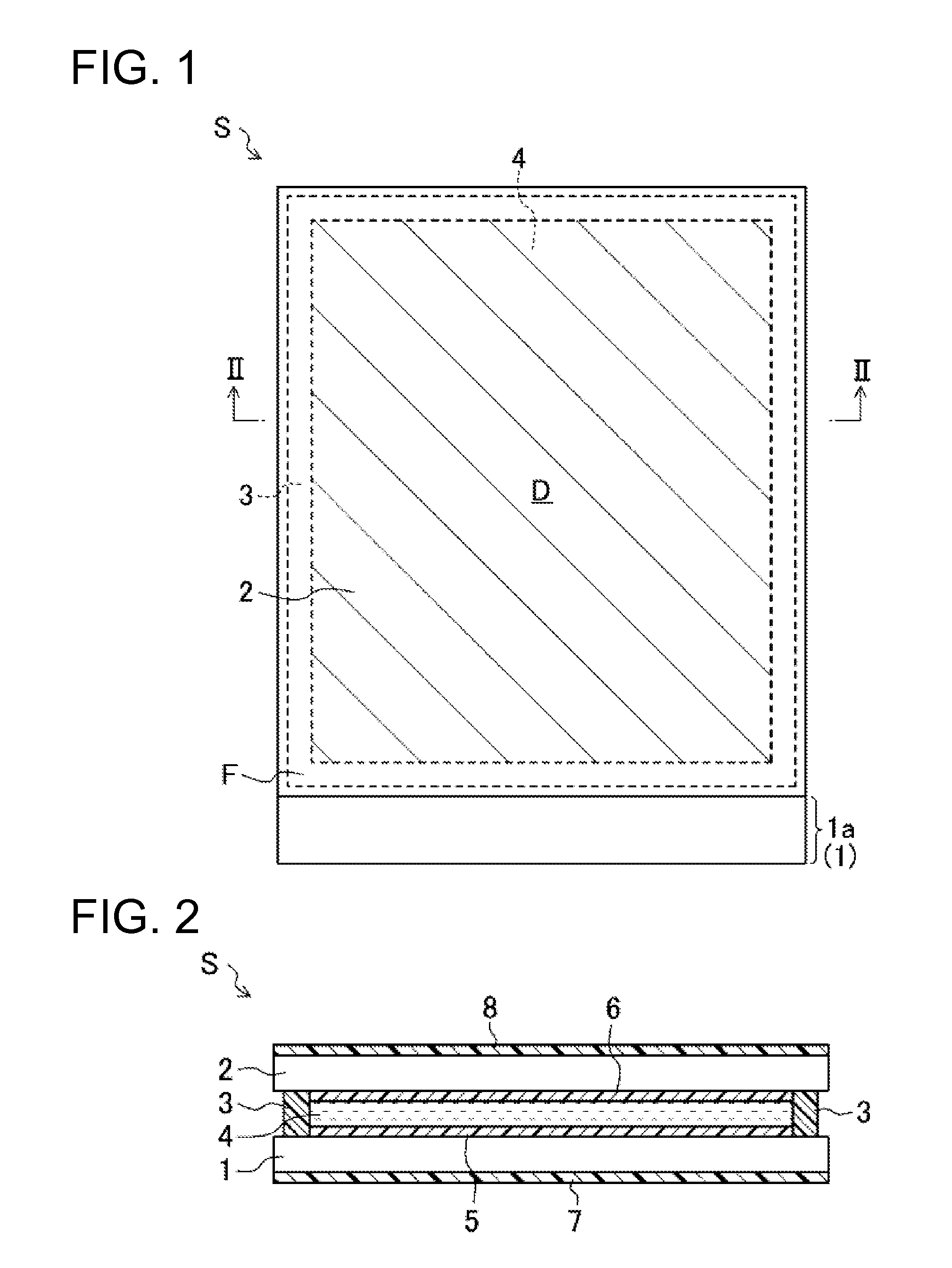
[0068]The configuration of the liquid crystal display device S is shown in FIGS. 1 and 2. FIG. 1 is a schematic plan view of the liquid crystal display device S. FIG. 2 is a schematic cross-sectional view showing a cross-sectional structure along the line II-II of FIG. 1.

[0069]

[0070]As shown in FIGS. 1 and 2, the liquid crystal display device S is provided with an active matrix substrate 1 that is a semiconductor device of the present invention, an opposite substrate 2 disposed to face the active matrix substrate 1, a frame-shaped sealing member 3 that bonds respective outer edges of the active matrix substrate 1 and the opposite substrate 2, and a liquid crystal layer 4 surrounded by the sealing member 3 and sealed between the active matrix su...

modification example of embodiment 1

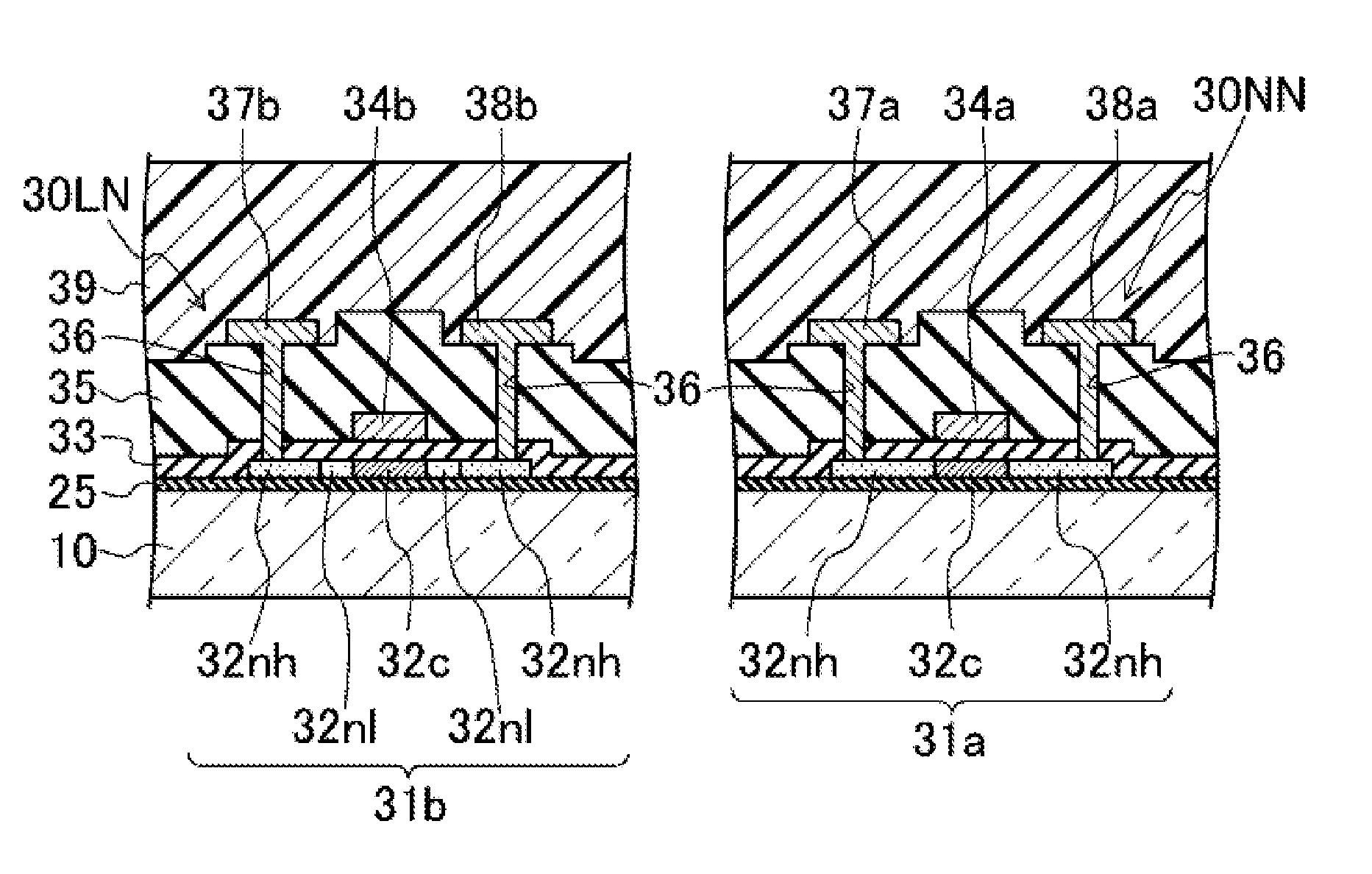
[0167]FIG. 15 shows, on the left side thereof, a cross-sectional view illustrating a cross-sectional structure of an n-type TFT 30ON of the offset structure according to this modification example. On the right side of FIG. 15, the n-type TFT 30NN of the normal structure, similar to that in Embodiment 1 above, is shown.

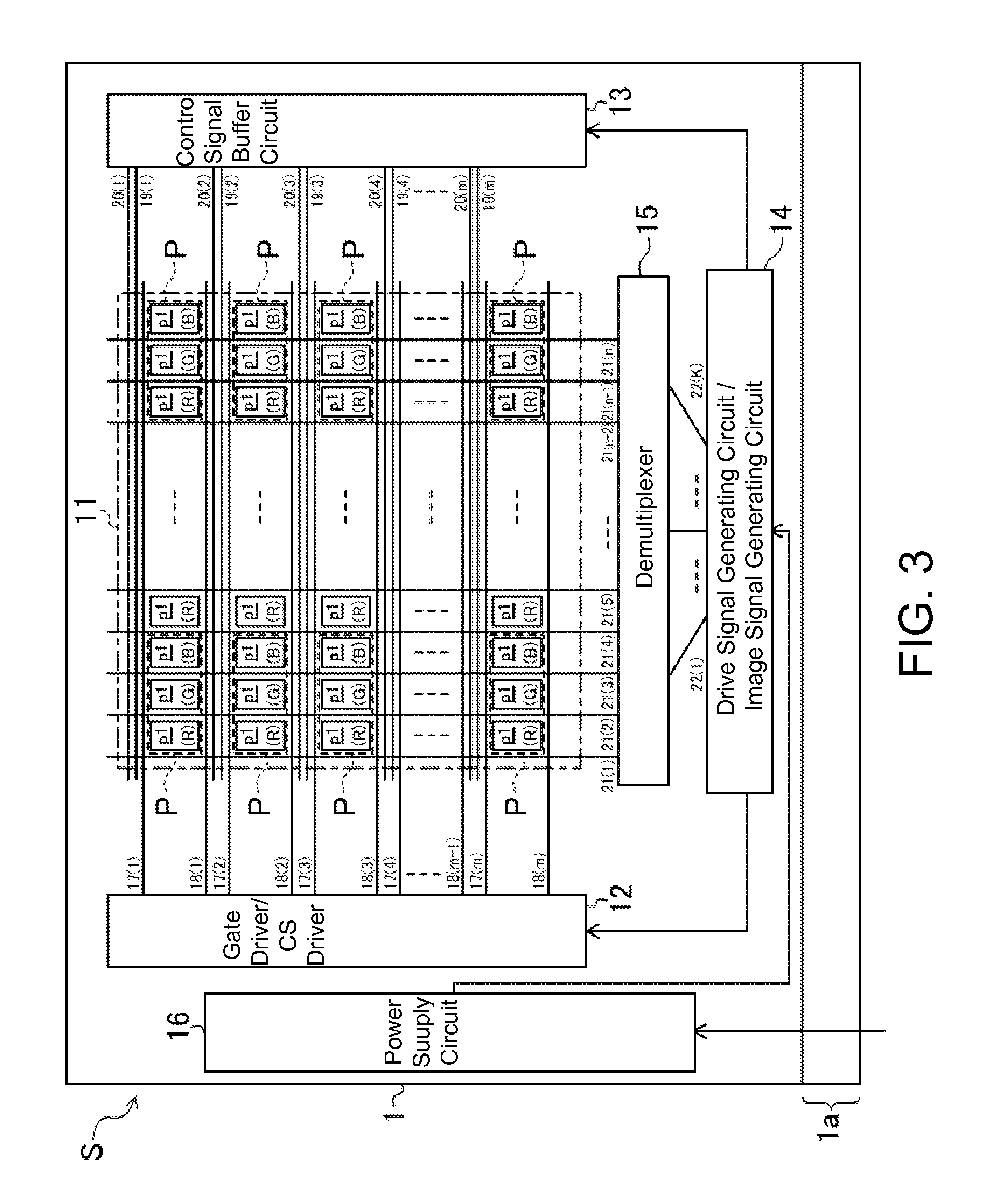
[0168]In this modification example, the switching TFT in each subpixel p1 is constituted of the n-type TFT 30ON of the offset structure, instead of the n-type TFT 30LN of the LDD structure, and the respective drive control circuits (the gate driver / CS driver 12, the control signal buffer circuit 13, and the drive signal generating circuit / image signal generating circuit 14) also include similar n-type TFTs 30ON of the offset structure. In other words, in the active matrix substrate 1 of this modification example, the n-type TFT 30ON of the offset structure and the n-type TFT 30NN of the normal structure are formed on the same substrate.

[0169]In a manner similar to the ...

embodiment 2

[0188]FIG. 18 show cross-sectional views of portions of an active matrix substrate 1 of Embodiment 2. In the figure, an n-type TFT 30LN of the LDD structure is shown in the left side, an n-type TFT 30NN of the normal structure is shown in the center, and a p-type TFT 3ONP of the normal structure is shown in the right side, respectively.

[0189]The present embodiment is configured in a manner similar to Embodiment 1 above, except for TFTs included in the power supply circuit 16, a memory circuit, and the respective drive control circuits (the gate driver / CS driver 12, the control signal buffer circuit 13, and the drive signal generating circuit / image signal generating circuit 14), and therefore, TFTs included in the power supply circuit 16, the memory circuit, and the respective drive control circuits 12, 13, and 14 will only be explained. In the embodiments below, the same configurations as those in FIGS. 1 to 17 are given the same reference characters and the same descriptions as tho...


PUM


Abstract

A first resist layer (46a) and a second resist layer (46b) that is thicker than the first resist layer (46a) are formed using a multi-gradient mask, a conductive film (44) is isotropically etched with both resist layers (46a, 46b) as masks, gate electrodes (34a, 34b) are formed narrower than the resist layers (46a, 46b) at locations corresponding to first and second semiconductor layers (31a, 31b), overhang portions (47) of the resist layers (46a, 46b) are configured at the sides of the gate electrodes (34a, 34b), then the entire first resist layer (46a) is removed and the second resist layer (46b) is thinned into a thin film; and an impurity is injected into the first semiconductor layer (31a) with the gate electrode (34b) as a mask, and into the second semiconductor layer (31b) with the second resist layer (46b) as a mask.

Description

TECHNICAL FIELD[0001]The present invention relates to a manufacturing method for a semiconductor device, and more particularly, to a reduction in the number of photomasks and manufacturing steps in forming, on the same substrate, a thin film transistor (referred to as a TFT below) of an LDD (lightly doped drain) structure or an offset structure and a TFT of a normal structure that does not have the LDD structure or offset structure.BACKGROUND ART[0002]Various display devices such as an active matrix driving type liquid crystal display device and an organic EL (electroluminescence) display device generally have a display region in which a plurality of pixels, each of which is the smallest unit of an image, are arranged in a matrix, and an active matrix substrate in which a switching TFT is provided for each pixel as a semiconductor device.[0003]When forming a semiconductor layer of the TFT by using amorphous silicon (a-Si), because of a relatively small carrier mobility of the amorph...

Claims


Application Information

Patent Timeline
Patent Type & Authority Applications(United States)
IPC IPC(8): H01L21/04
CPCH01L21/04H01L27/1288H01L29/78621H01L29/66757G02F1/136236
Inventor SAITOH, MASAKI
Owner SHARP KK
Why Eureka
Try Eureka