Method and Apparatus for a Large Area Inductive Plasma Source

Inactive Publication Date: 2014-03-06
MKS INSTR INC
View PDF2 Cites 143 Cited by
  • Summary
  • Abstract
  • Description
  • Claims
  • Application Information

AI Technical Summary

Benefits of technology

[0010]One advantage of the invention is that ionized and/or activated gaseous species are substantially uniformly distributed within a process chamber, and can be distributed over a large area within the process chamber. Another advantage is that activated species generated by the plasma, such as ions, atoms, and excited molecules, can flow to the process chamber and substrate surfaces within a short time after they are produced, minimizing the losses of the activated species during transport. Minimizing losses of activated species during transport is important for gases with a short half-life (e.g., on the order of a millisecond or less). For example, atomic hydrogen, atomic chlorine, and atomic nitrogen each have a half-life that can be a millisecond or less.
[0011]Another advantage of the invention is that the distance between the plasma and the substrate to be processed within the semiconductor process chamber is substantially equal for each outlet from the toroidal plasma chamber into the semiconductor processing chamber, as the toroidal plasma is in parallel with the substrate surface. The lifetimes of the ions and various activated neutral species can be very different. The composition of the gaseous species therefore changes with the distance from plasma source. Orienting the plasma source in parallel with the substrate surface can result in the chemical compositions of the process gases being approximately uniform across the substrate surface.
[0012]In one aspect, the invention includes a plasma source for providing dissociated gas to semiconductor process chamber. The plasma source includes a plasma chamber having at least one gas inlet, at least one chamber wall for containing the gas, and at least one outlet into the semiconductor process chamber. The plasma source also includes a plurality of magnetic cores disposed relative to the plasma chamber such that the plasma chamber pass

Problems solved by technology

For example, some applications require the use of ions with low kinetic energy (i.e. a few electron volts) because the material being processed is sensitive to damage.
However, some RF inductively coupled plasmas are not purely inductive because the drive currents are only weakly coupled to the plasma.
Consequently, RF inductively coupled plasmas are often inefficient and require the use of high voltages on the drive coils.
The ion bombardment deteriorates the reactor and can contaminate

Method used


Image

  • Method and Apparatus for a Large Area Inductive Plasma Source
  • Method and Apparatus for a Large Area Inductive Plasma Source
  • Method and Apparatus for a Large Area Inductive Plasma Source

Examples


Example

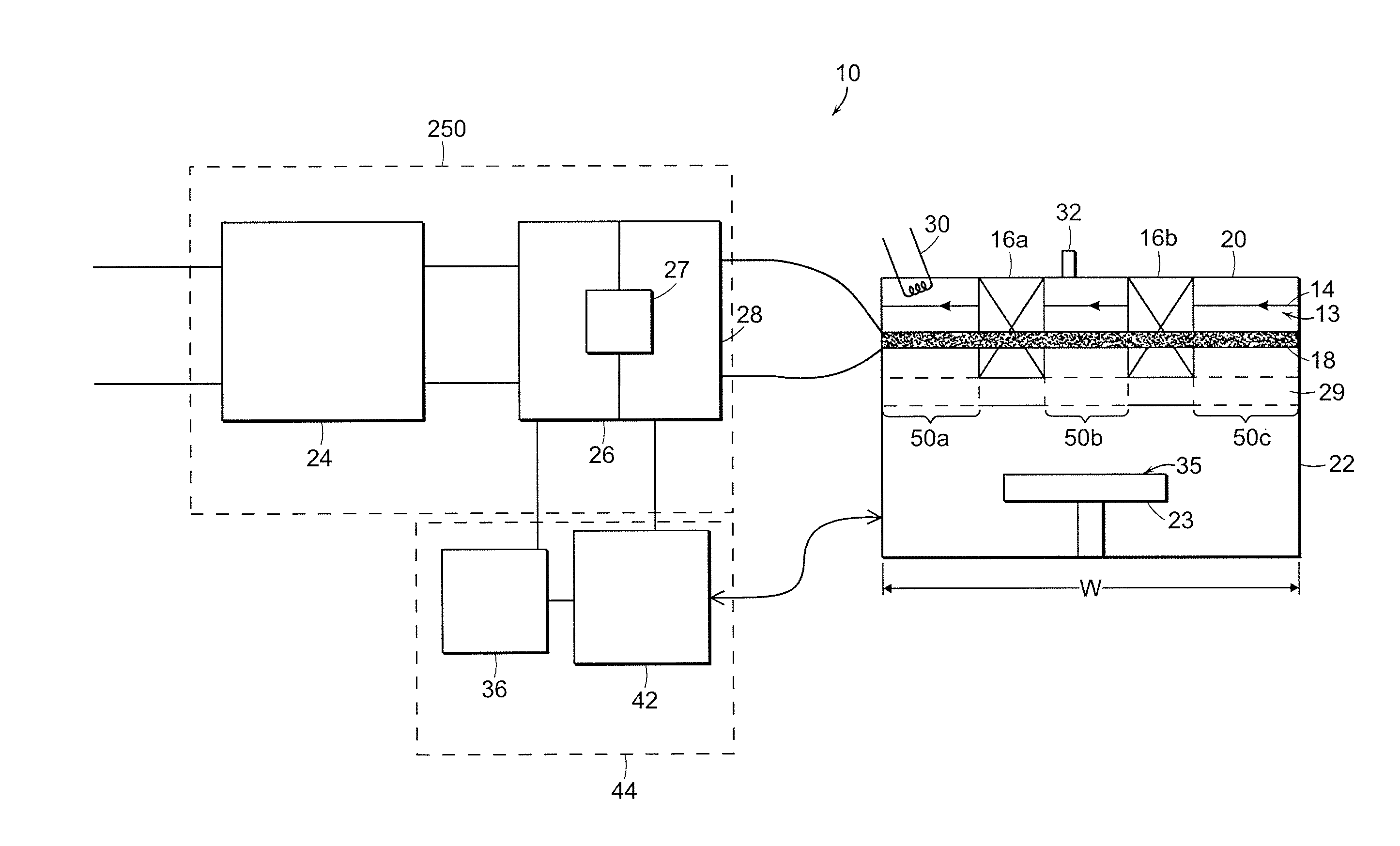
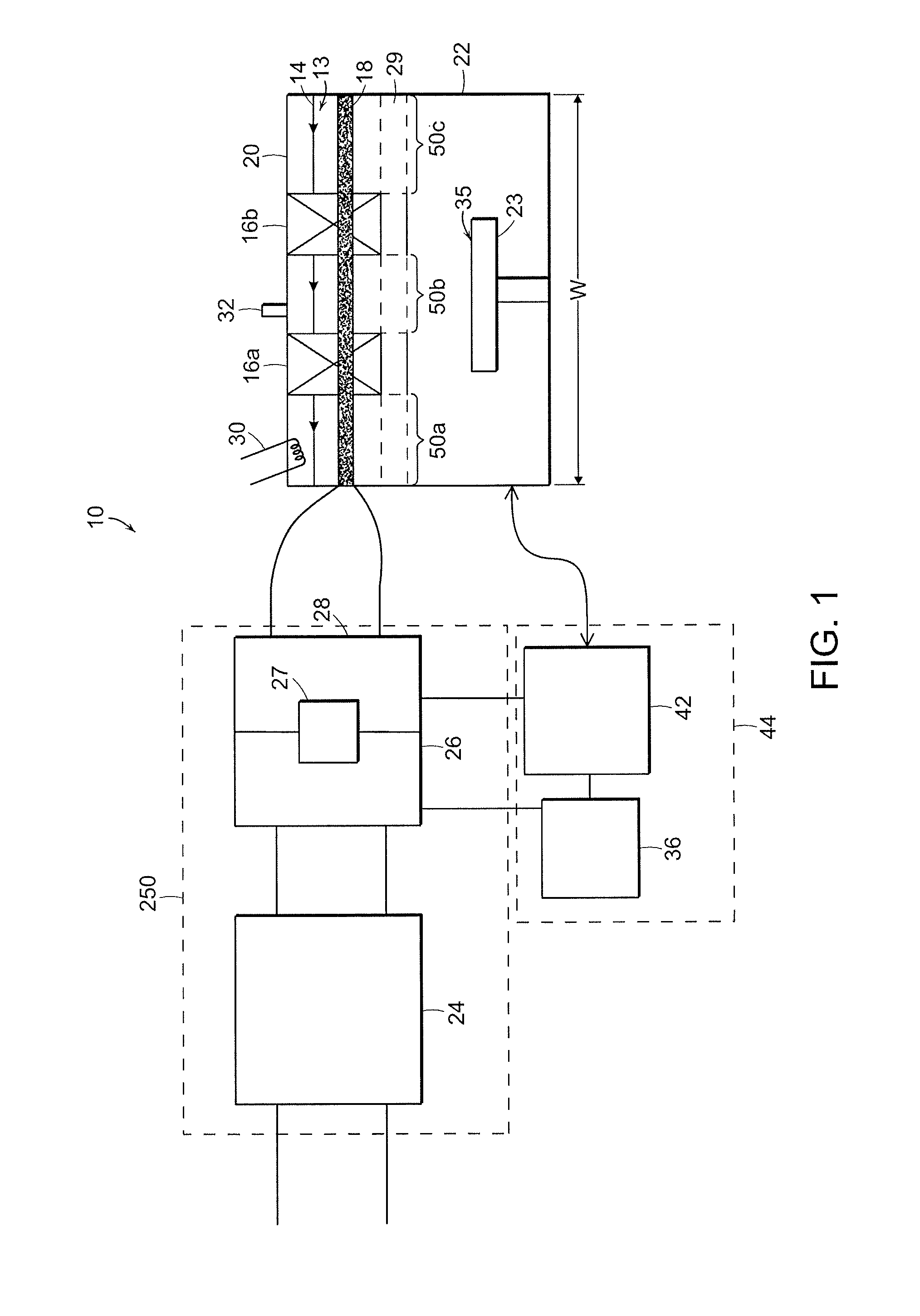
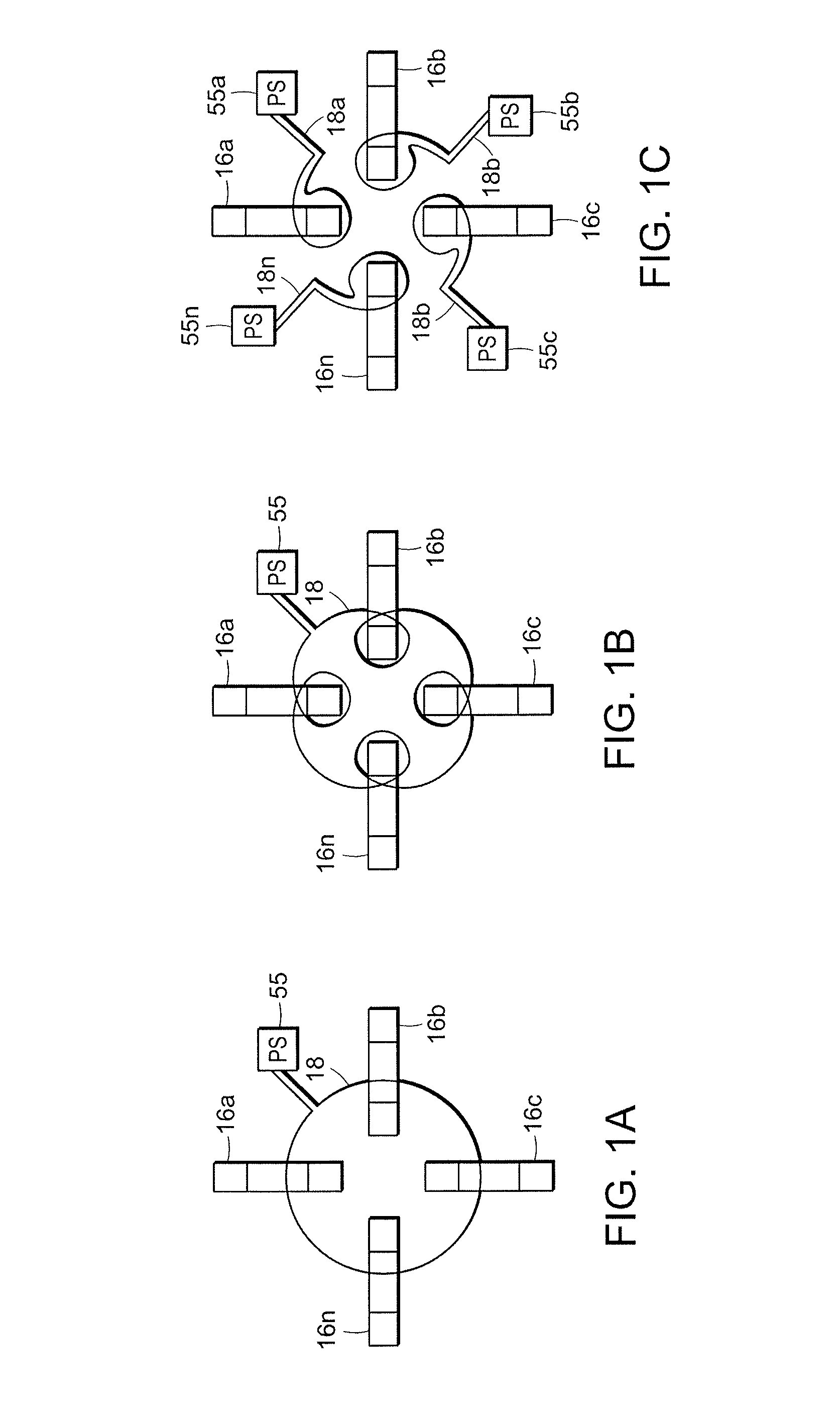
[0040]The present invention features a plasma source for use during semiconductor processing. The plasma source includes one or more toroidal plasma chambers. Each toroidal plasma chamber is configured to contain a plasma loop formed within such chamber. The one or more toroidal plasma chambers are coupled to a process chamber such that each plasma loop is oriented substantially parallel to a substrate holder disposed within the process chamber. A plasma loop having a parallel orientation relative to the substrate holder allows a larger area of a substrate to be processed by the activated gases and provides a more even distribution of the activated gases on the surface of the substrate to be processed.

[0041]Some embodiments of the invention feature a plasma source that is coupled to a lid of a semiconductor process chamber. The plasma source can include multiple magnetic cores and a toroidal plasma chamber that passes through the multiple magnetic cores. The plasma source can be cou...


PUM


Abstract

A plasma source for providing dissociated gas to semiconductor process chamber is provided. The plasma chamber can have at least one gas inlet and at least one chamber wall for containing the gas, a plurality of magnetic cores disposed relative to the plasma chamber such that the plasma chamber passes through each of the plurality of magnetic cores. A primary winding can be coupled to the plurality of magnetic cores. The plasma chamber can generate a toroidal plasma along a plane extending through the plasma chamber and which is at least substantially parallel to a top surface of a sample holder disposed within the semiconductor process chamber.

Description

FIELD OF THE INVENTION[0001]This invention relates generally to the field of generating activated gas containing ions, free radicals, atoms, and molecules, and to apparatuses for and methods of processing materials with activated gas.BACKGROUND OF THE INVENTION[0002]Plasma discharges can be used to excite gases to produce activated gases containing ions, free radicals, atoms and molecules. Activated gases are used for numerous industrial and scientific applications including processing solid materials such as semiconductor wafers, powders, and other gases. The parameters of the plasma and the conditions of the exposure of the plasma to the material being processed vary widely depending on the application.[0003]For example, some applications require the use of ions with low kinetic energy (i.e. a few electron volts) because the material being processed is sensitive to damage. Other applications, such as ion implementation, anisotropic etching or planarized dielectric deposition, requ...

Claims


Application Information

Patent Timeline
IPC IPC(8): H05H7/04H05H1/24
CPCH05H1/24H05H7/04H01J37/321H01J37/3266H01J37/32669
Inventor CHEN, XING
Owner MKS INSTR INC
Why Eureka
Try Eureka