Circuitry and method for reducing area and power of a pipeline ADC

a technology of pipeline adc and circuit, which is applied in the field of circuitry and method for reducing the area and power of pipeline adc, can solve the problems of inconvenient design, inconvenient design, and insufficient preamplifier stage in each comparator, so as to reduce the number of comparators, reduce the difficulty of designing, and reduce the area of integrated circuit chip area and power dissipation

Active Publication Date: 2014-03-06
TEXAS INSTR INC
View PDF0 Cites 14 Cited by
  • Summary
  • Abstract
  • Description
  • Claims
  • Application Information

AI Technical Summary

Benefits of technology

[0013]There also is an unmet need for an accurate, linear pipeline ADC which avoids problems associated with pipeline ADCs that utilize reference scaling.
[0014]There also is an unmet need for a technique for reducing the difficulty of designing the components of a high-resolution pipeline ADC.
[0015]It is an object of the invention to provide an accurate, linear pipeline ADC and method which require substantially less integrated circuit chip area and power dissipation than prior pipeline ADCs that have otherwise essentially similar perf

Problems solved by technology

Various errors generated in the known pipeline ADCs cause nonlinear operation thereof.
One source of error is random input offset voltages of the flash comparators of the various stages.
Another source of error is random input-referred input offset voltages of the residue amplifiers of the various stages.
Yet another, error is due to variations in the series-connected resistors of the flash ADCs.
The preamplifier stage in each comparator requires undesirably large amounts of additional chip area and power dissipation.
This limitation is especially large for ADCs having higher than 10-bit resolution.
A “cost” or drawback of using a redundancy bit in a pipeline ADC stage is that the number of flash ADC comparators in the pipeline ADC stage must be doubled.
Unfortu

Method used


Image

  • Circuitry and method for reducing area and power of a pipeline ADC
  • Circuitry and method for reducing area and power of a pipeline ADC
  • Circuitry and method for reducing area and power of a pipeline ADC

Examples


Embodiment Construction

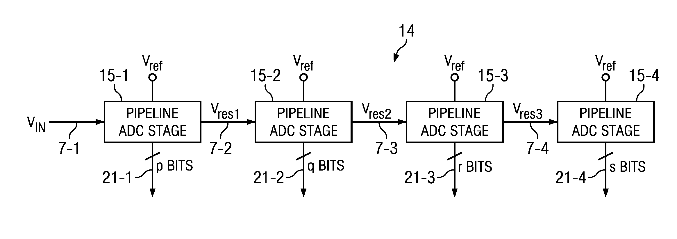
[0046]An improvement to conventional “pipeline ADC stages” for a pipeline ADC is provided which avoids the need to double the number of flash ADC comparators of a “next” pipeline ADC stage when redundancy bits are used to improve the linearity of the pipeline ADC. The improvement is accomplished by using residue voltage level detecting circuitry which detects an out-of-range excursion of the residue voltage and accordingly provides feedback that shifts the residue voltage back into the desired range for each pipeline ADC stage following the first stage.

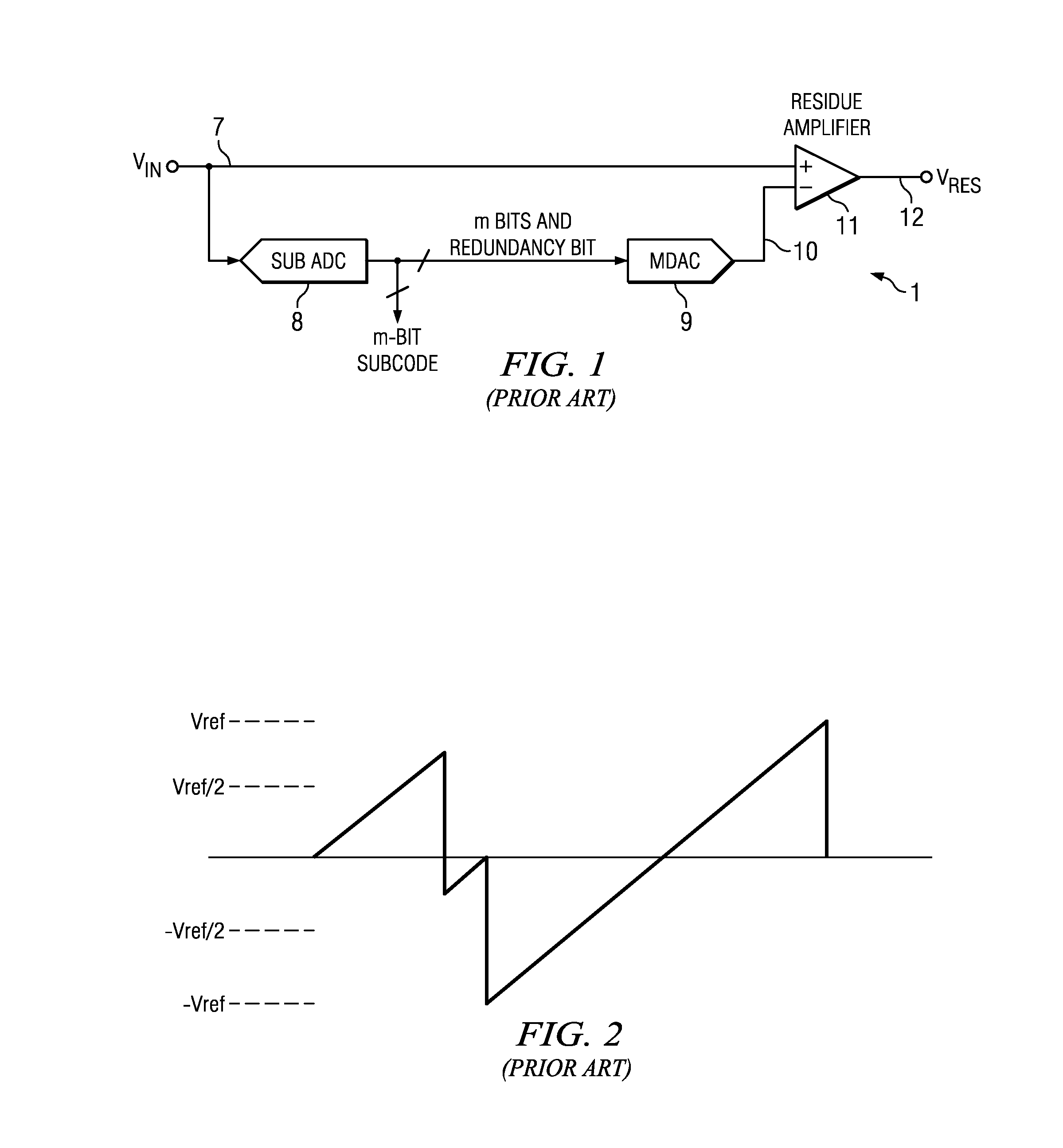
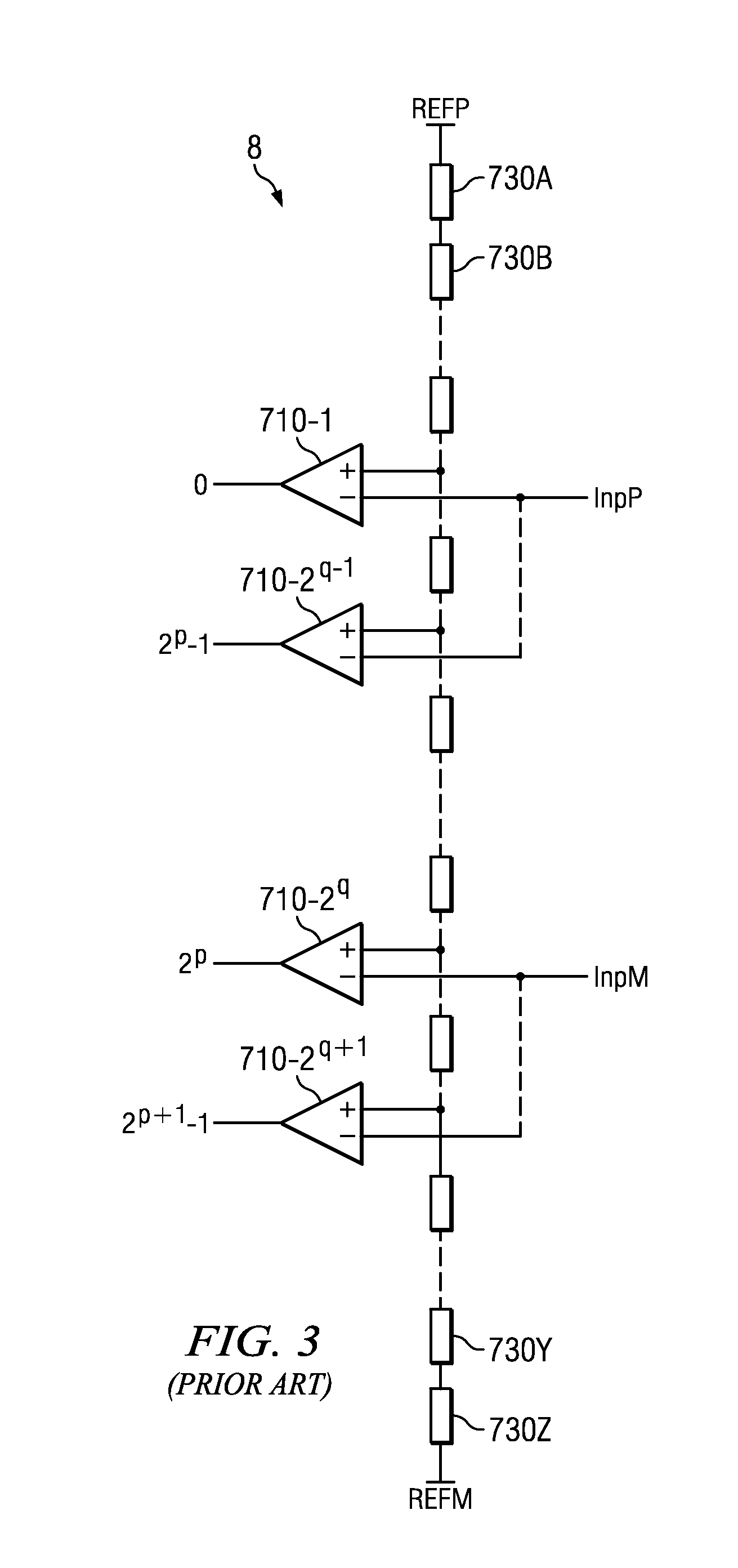
[0047]FIG. 4A shows a new pipeline ADC stage 15 wherein analog input signal VIN (which typically is the residue voltage of a previous pipeline ADC stage) is applied by conductor 7 to the input of a sub-ADC 8 and also to the (+) input of a residue amplifier 11A. Sub-ADC 8 may be implemented by means of a flash ADC 8, which is commonly used in conventional pipeline ADCs. Flash ADC 8 in FIG. 4A is similar to the one shown in Prior Art FI...


PUM


Abstract

A pipeline ADC (analog-to-digital converter) (14) includes a residue amplifier (7) for applying a first residue signal (Vres1) to a first input of a residue amplifier (11A) and to an input of a sub-ADC (8) for resolving a predetermined number (m) of bits and producing a redundancy bit in response to the first residue signal. A level-shifting MDAC (9A) converts the predetermined number of bits and the redundancy bit to an analog signal (10) on the a second input of the residue amplifier, which amplifies the difference between the first residue signal and the analog signal to generate a second residue signal (Vres2). The MDAC causes the residue amplifier to shift the second residue signal back within a predetermined voltage range (±Vref/2) by the end of the amplifying if the second residue signal is outside of the predetermined voltage range.

Description

BACKGROUND OF THE INVENTION[0001]The present invention relates generally to improvements which increase the linearity of pipeline ADCs (analog-to-digital converters), and more particularly to improvements which substantially reduce the number of “next stage comparators” in the pipeline ADC. The invention relates yet more particularly to improvements which also reduce the amount of integrated circuit chip area and power dissipation compared to that of prior pipeline ADCs.[0002]A pipeline ADC includes a sequence of pipeline ADC “stages”. FIG. 1 shows a single conventional pipeline ADC stage 1 wherein an analog input signal VIN is applied by conductor 7 to the input of a sub-ADC 8 and to the (+) input of a residue amplifier 11. Sub-ADC 8 typically is implemented by means of a flash ADC. The digital output of sub-ADC 8 is applied to the input of a conventional multiplier DAC (MDAC) 9, the output of which is applied to the (−) input of residue amplifier 11, which produces a residue volta...

Claims


Application Information

Patent Timeline
IPC IPC(8): H03M1/12H03M1/00
CPCH03M1/0675H03M1/167H03M1/1009H03M1/12H03M1/10H03M1/164
Inventor NANDI, GAUTAM S.KHURANA, RISHUBH
Owner TEXAS INSTR INC
Why Eureka
Try Eureka