Capacitive touch panel with force sensing

a touch panel and force sensing technology, applied in the field of capacitive touch panel devices, can solve the problems of reducing the cost and complexity of additional devices, and achieve the effects of reducing the cost and complexity, improving spatial resolution, sensitivity, and mechanical robustness

Active Publication Date: 2014-03-06
SHARP KK
View PDF10 Cites 170 Cited by
  • Summary
  • Abstract
  • Description
  • Claims
  • Application Information

AI Technical Summary

Benefits of technology

[0012]The capacitive touch sensing device in accordance with the present invention overcomes the aforementioned limitations of current touch sensing devices. Firstly, as no electrical connection need be made to the second array, additional cost and complexity is minimised. Secondly, as the additional electrode layer resides near the top of the device structure, the lower layers of the structure need not be deformed upon application of an external touch force. This improves spatial resolution, sensitivity, and mechanical robustness. Furthermore, the new sensor structure is compatible with conventional controller circuits.

Problems solved by technology

Firstly, as no electrical connection need be made to the second array, additional cost and complexity is minimised.

Method used


Image

  • Capacitive touch panel with force sensing
  • Capacitive touch panel with force sensing
  • Capacitive touch panel with force sensing

Examples


first embodiment

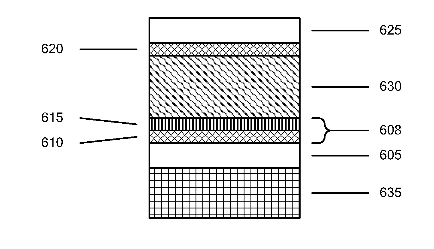
[0099]A touch sensing device in accordance with the present invention is shown in FIG. 4. A first electrode array comprising drive electrodes 610 and sense electrodes 615 is formed in first electrode layer 608 on a first sensor substrate 605. The drive and sense electrodes are electrically insulated from one another, and may be similar to those found in a conventional projected capacitance touch sensor. A second electrode array of electrically separate conductive regions is formed in a second electrode layer 620 on a second substrate 625. The second electrode layer 620 is separated from the first electrode layer 608 by a deformable medium 630. The first array and second array of may be formed, for example, by patterning a layer of transparent conductive material—such as indium tin oxide (ITO) or the like—using standard photolithographic or printing processes. The first sensor substrate and second substrate 625 may be made of a transparent material such as, for example, glass or plas...

second embodiment

[0113]In a touch sensing device in accordance with the invention each sense electrode in the first electrode array is symmetrically divided along its principal direction into a first sense electrode section and a second sense electrode section. The conductive regions of the second electrode array are patterned and aligned so as to overlap at least partially the drive electrodes, to overlap at least partially the first sense electrode section of a sense electrode, but not to overlap the second sense electrode section. FIG. 12 shows a plan view the first substrate 605 illustrating an exemplary arrangement of the first electrode array with a diamond patterned sense electrode divided into two sense electrode sections. Also shown is the second electrode array of conductive regions 902 formed in the second electrode layer on the second substrate (not shown for clarity). Here the first sense electrode section 1210 does not lie beneath the conductive regions 902, yet the second sense electr...

fourth embodiment

[0117]In the present invention, the sense electrodes are divided into two sections that share a common geometric centroid. FIG. 14 is a plan view of an exemplary first and second electrode array in accordance with the present embodiment. Here, the sense electrodes 720 are divided into a first ring section 1410 and a second centre section 1420. The first ring section 1410 is arranged symmetrically around the second centre section 1420 such that the two sections share a common centroid. Floating conductive regions 902, formed in the second electrode layer on the second substrate, are patterned so as to overlap at least partially the drive electrodes 710, overlap at least partially the ring section 1410 of a sense electrode but not to overlap the centre section 1420 of a sense electrode. The ring section 1410 of the sense electrode therefore forms the force sensing intersection with the drive electrode, and the centre section 1420 of the sense electrode forms the touch sensing intersec...


PUM


Abstract

A capacitive type touch sensing device includes a first electrode array including a plurality of drive electrodes and a plurality of sense electrodes, and a second electrode array spaced apart from the first electrode array and including a plurality of discrete, electrically floating conductive regions. At least part of the second electrode array positionally overlaps with at least part of the first electrode array to define a separation distance therebetween, the separation distance varying with a force applied to a surface of the touch sensing device. Further, each conductive region is positioned relative to a respective drive electrode and sense electrode of the first electrode array so that a capacitance between certain pairs of drive and sense electrodes is more sensitive to a variation in the separation distance than a capacitance between other pairs of drive and sense electrodes.

Description

TECHNICAL FIELD AND APPLICATIONS OF THE INVENTION[0001]The present invention relates to touch panel devices and, more particularly, to capacitive type touch panels. A capacitive type touch panel device may find application in a range of consumer electronic products including, for example, mobile phones, tablet and desktop PCs, electronic book readers and digital signage products.BACKGROUND ART[0002]Touch panels have recently become widely adopted as the input device for high-end portable electronic products such as smart-phones and tablet devices. Although, a number of different technologies can be used to create these touch panels, capacitive systems have proven to be the most popular due to their accuracy, durability and ability to detect touch input events with little or no activation force.[0003]The most basic method of capacitive sensing for touch panels is demonstrated in surface capacitive systems, for example as disclosed in U.S. Pat. No. 4,293,734 (Pepper, Oct. 6, 1981). A ...

Claims


Application Information

Patent Timeline
Patent Type & Authority Applications(United States)
IPC IPC(8): G06F3/044
CPCG06F3/0445G06F3/0447G06F2203/04105
Inventor COULSON, MICHAEL PAULBROWN, CHRISTOPHER JAMESSLAMKUL, DAUREN
Owner SHARP KK
Why Eureka
Try Eureka