Integrated circuit including an environmental sensor

a technology of integrated circuits and sensors, applied in the direction of microelectromechanical systems, semiconductor devices, semiconductor/solid-state device details, etc., can solve the problems of difficult to control the exact position of the opening b, sensitive sensor features such as the deflectable membrane of a pressure sensor, and the inability to use a relatively large portion of substrates, etc., to achieve convenient manufacturing of integrated circuits, enhance the ability of elongation channels, and optimize matching

Active Publication Date: 2014-03-13
SCIOSENSE BV
View PDF5 Cites 22 Cited by
  • Summary
  • Abstract
  • Description
  • Claims
  • Application Information

AI Technical Summary

Benefits of technology

[0027]In another embodiment the cap layer can be formed from a second semiconductor substrate. The second substrate can comprise the same material as the first substrate (e.g. Si) so as to provide optimal matching of similar thermal expansion characteristics. The second substrate can be patterned using standard lithographic etching techniques for producing features such as the at least one elongate channel and/or the at least one cavity that adjoins an area of the major surface. The second substrate can, for example, be attached to the semiconductor substrate including the at least one environmental sensor using techniques such as fusion bonding or eutectic bondin

Problems solved by technology

However, environmental sensors such as pressure sensors or gas sensors require direct access to the environment surrounding the integrated circuit to perform their sensing function.
For example, when using the foil assisted moulding process, it is difficult to control the exact position of the opening 8.
Because of this lack of positional accuracy, a relatively large portion of substrate cannot be used.
Also, since the environmental sensor 6 is left exposed throughout the manufacturing process, delicate features of the sensor (such as the deflectable membrane of a pressure sensor or the suspended resistive wire of a thermal conduc

Method used


Image

  • Integrated circuit including an environmental sensor
  • Integrated circuit including an environmental sensor
  • Integrated circuit including an environmental sensor

Examples


Embodiment Construction

[0044]Embodiments of the present invention are described in the following with reference to the accompanying drawings.

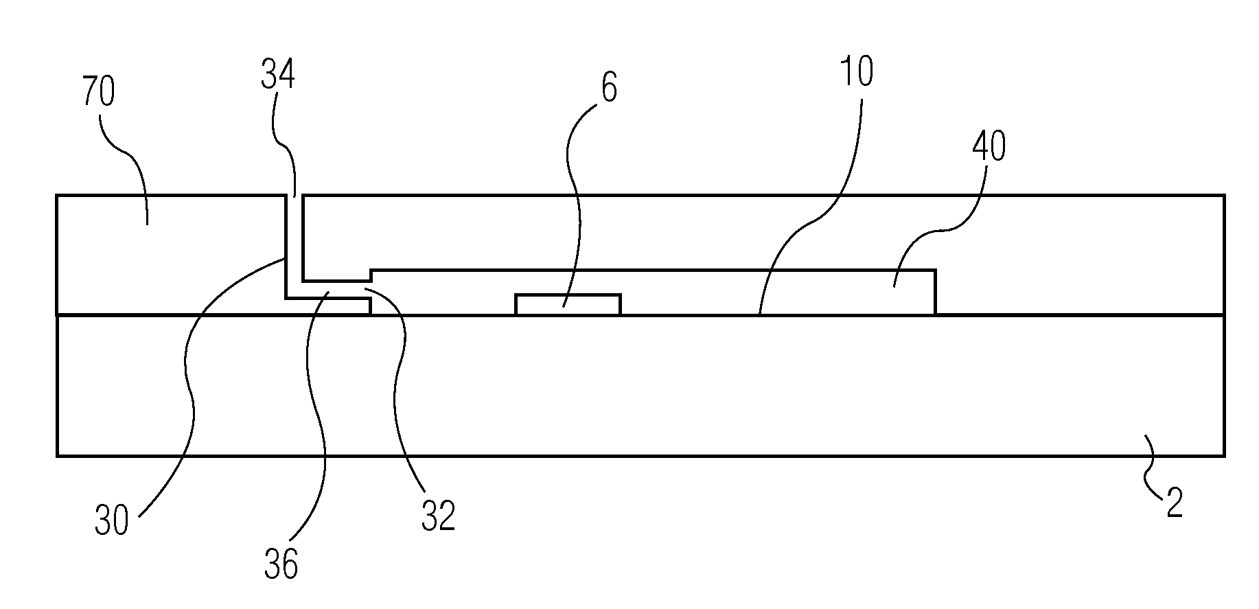
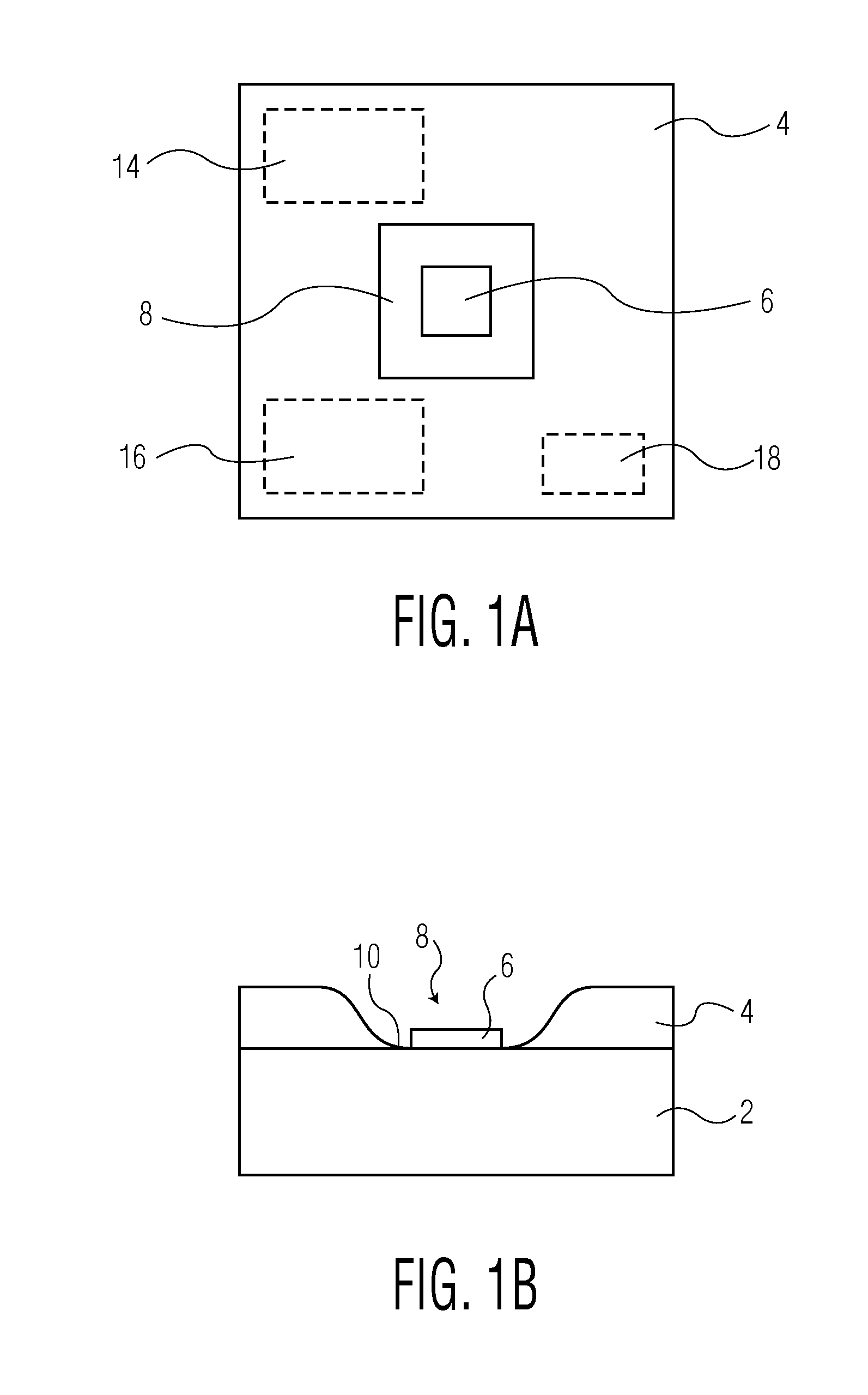
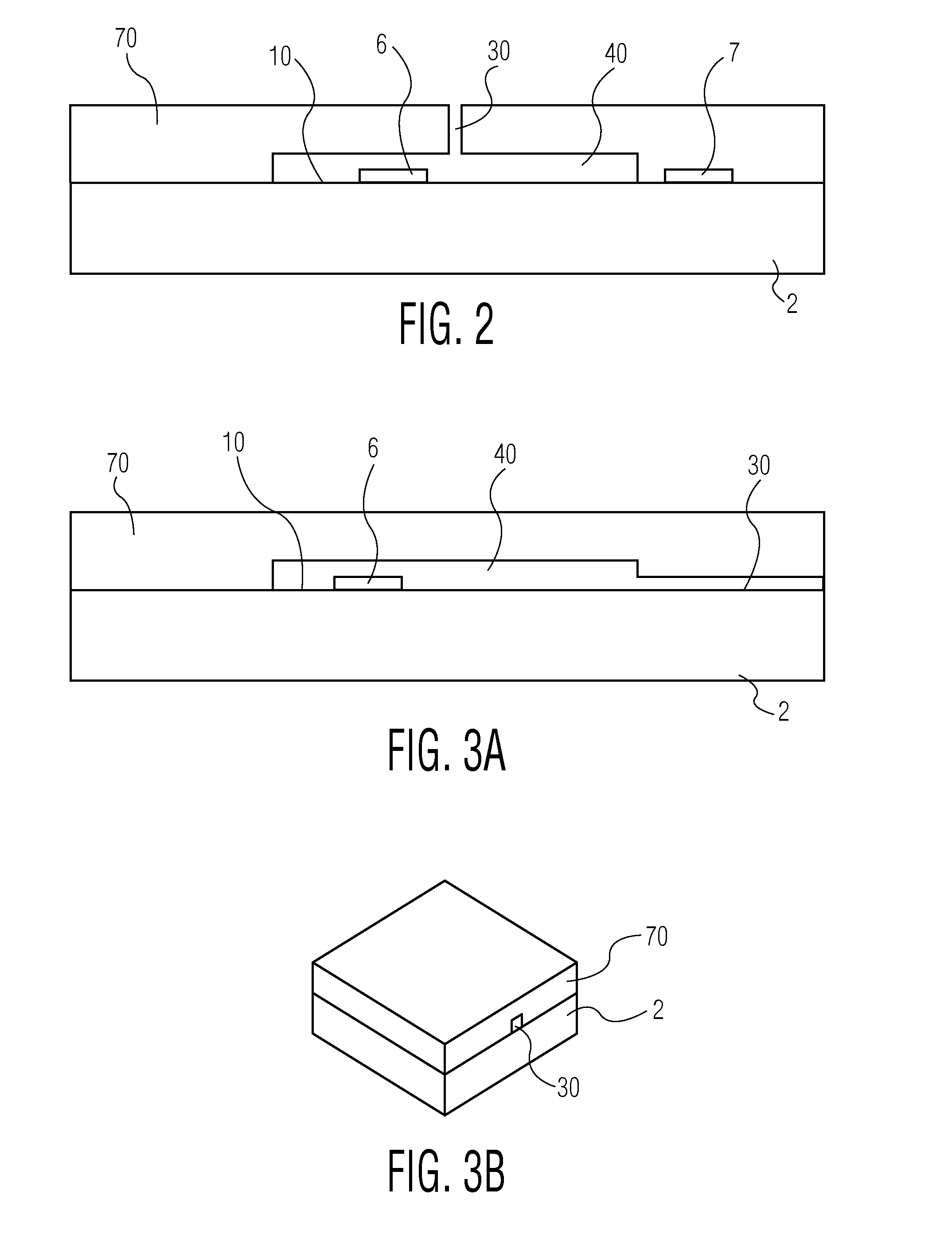
[0045]A first example of an integrated circuit in accordance with an embodiment of the invention is illustrated in FIG. 2. The integrated circuit includes a semiconductor substrate 2, which may comprise, for example, silicon. The semiconductor substrate 2 has a major surface 10. An environmental sensor 6 is provided on the major surface 10. The environmental sensor 6 is a sensor that requires direct physical access to the environment surrounding the integrated circuit in order correctly to perform its sensing function. Examples of such sensors include pressure sensors, gas sensors (for example CO2 sensors) humidity sensors, and pH sensors.

[0046]In addition to the environmental sensor 6, further components can also be provided in the semiconductor substrate 2. For example, there can be provided control circuitry for operating the environmental sensor 6, memory for sto...


PUM


Abstract

An integrated circuit and a method of making the same. The integrated circuit includes a semiconductor substrate including at least one environmental sensor. The integrated circuit also includes a cap layer located on a major surface of the substrate. The integrated circuit further includes at least one elongate channel for allowing access of said sensor to an environment surrounding the integrated circuit.

Description

BACKGROUND OF THE INVENTION[0001]This invention relates to an integrated circuit. In particular, this invention relates to an integrated circuit including at least one environmental sensor. The invention further relates to a method of making such an integrated circuit.[0002]Nowadays, integrated circuits may comprise a plethora of different sensors, such as ambient light (AL) sensors, temperature (T) sensors, pressure sensors, gas sensors, relative humidity (RH) sensors, specific analyte detection sensors, and so on.[0003]Integrated circuits of this kind have a wide range of applications. For example, they can be used in the field of supply chain management to track and monitor the freshness of food and beverages. They can also be used as environmental sensors, for example as part of a heating, ventilation and air conditioning (HVAC) system in an automobile or in a building (e.g. a Smart Building). Additional applications include those in agricultural (e.g. the sensing of environment...

Claims


Application Information

Patent Timeline
IPC IPC(8): H01L23/04H01L21/77
CPCH01L21/77H01L23/04B81B7/0061B81B2201/0264H01L21/50H01L23/3114H01L2924/0002
Inventor BESLING, WILLEM FREDERIK ADRIANUSKENGEN, MARTIEN
Owner SCIOSENSE BV
Why Eureka
Try Eureka