Bio-nanowire device and method of fabricating the same

a technology of nanowire and nanowire, which is applied in the field of nanowire devices, can solve the problems of unfavorable utilization of different functions through adjustment of operating conditions

Inactive Publication Date: 2014-03-20
NAT CHIAO TUNG UNIV
View PDF8 Cites 32 Cited by
  • Summary
  • Abstract
  • Description
  • Claims
  • Application Information

AI Technical Summary

Benefits of technology

[0018]wherein when a voltage or a current is applied to the bio-nanowires, the oxidation state of the metal ions

Problems solved by technology

However, nanostructured semiconductor devices fabricated using the aforementioned solid inorganic material, e.g., GaN, have fixed properties and limited applications (for instance, the semiconductor device di

Method used


Image

  • Bio-nanowire device and method of fabricating the same
  • Bio-nanowire device and method of fabricating the same
  • Bio-nanowire device and method of fabricating the same

Examples


Embodiment Construction

[0040]Before the present invention is described in greater detail, it should be noted that the same reference numerals have been used to denote like elements throughout the specification.

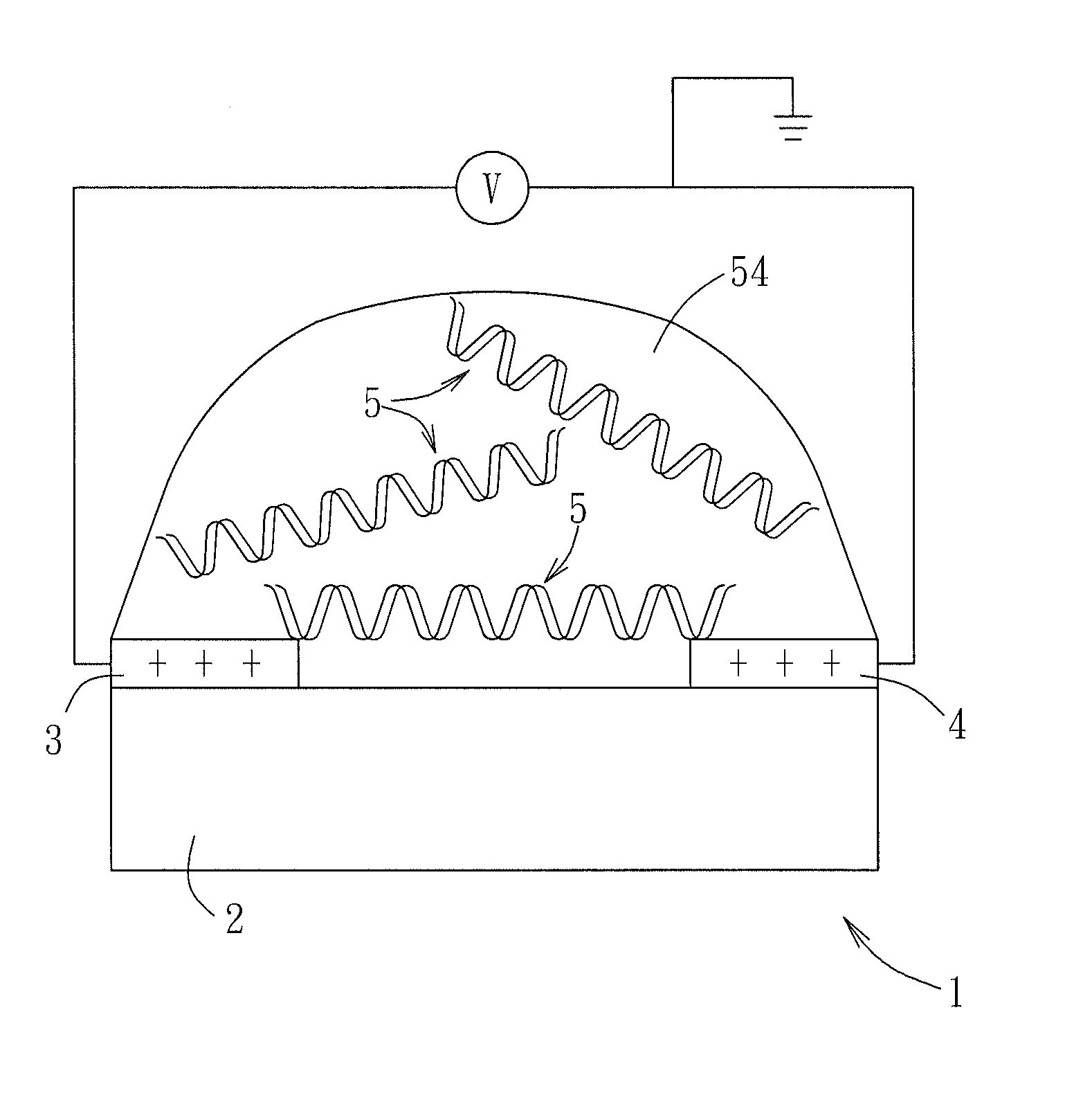
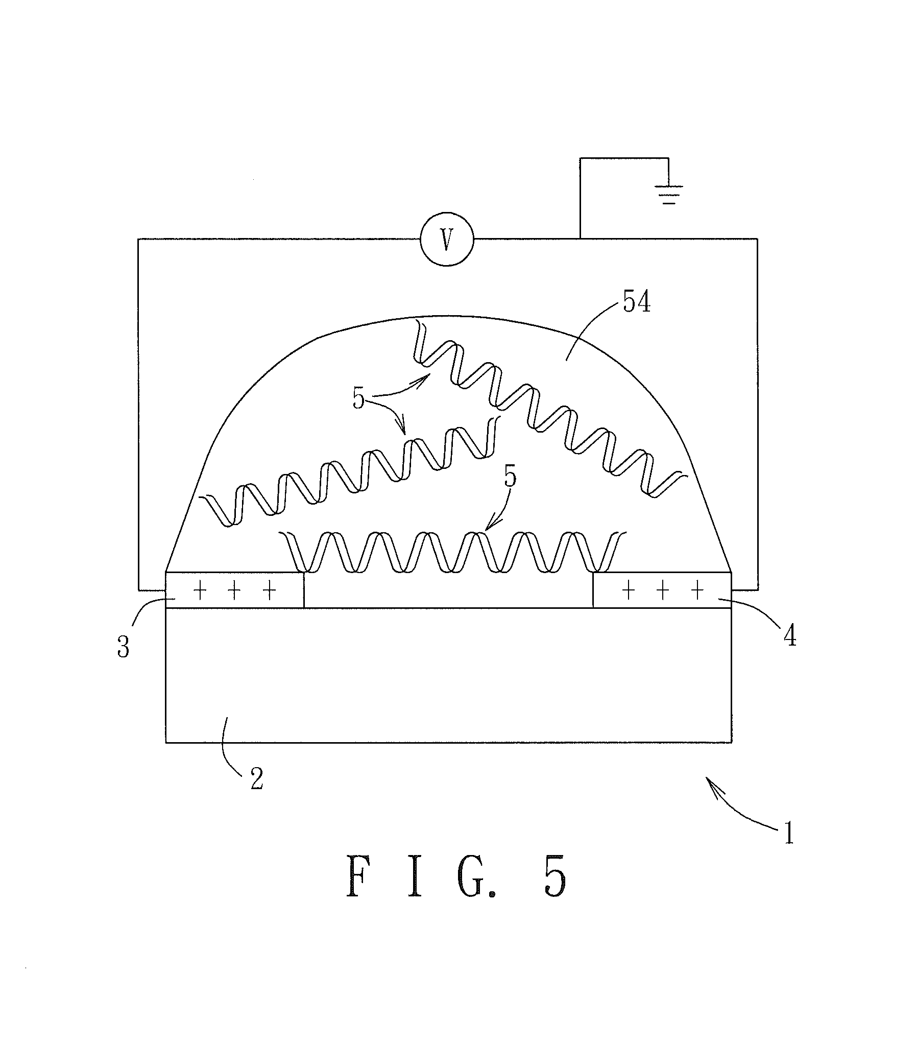
[0041]Referring to FIGS. 1 to 4, the first preferred embodiment of a bio-nanowire device 1 according to the present invention is shown. In the first preferred embodiment, by virtue of specific operating conditions (e.g., electric current, voltage, or magnetic field), the bio-nanowire device 1 can be controlled to perform different functions at different operating conditions. For example, under a corresponding operating condition, the bio-nanowire device 1 can perform a respective function so as to serve as a diode, a memristor, a spintronic device, or a bio-sensor.

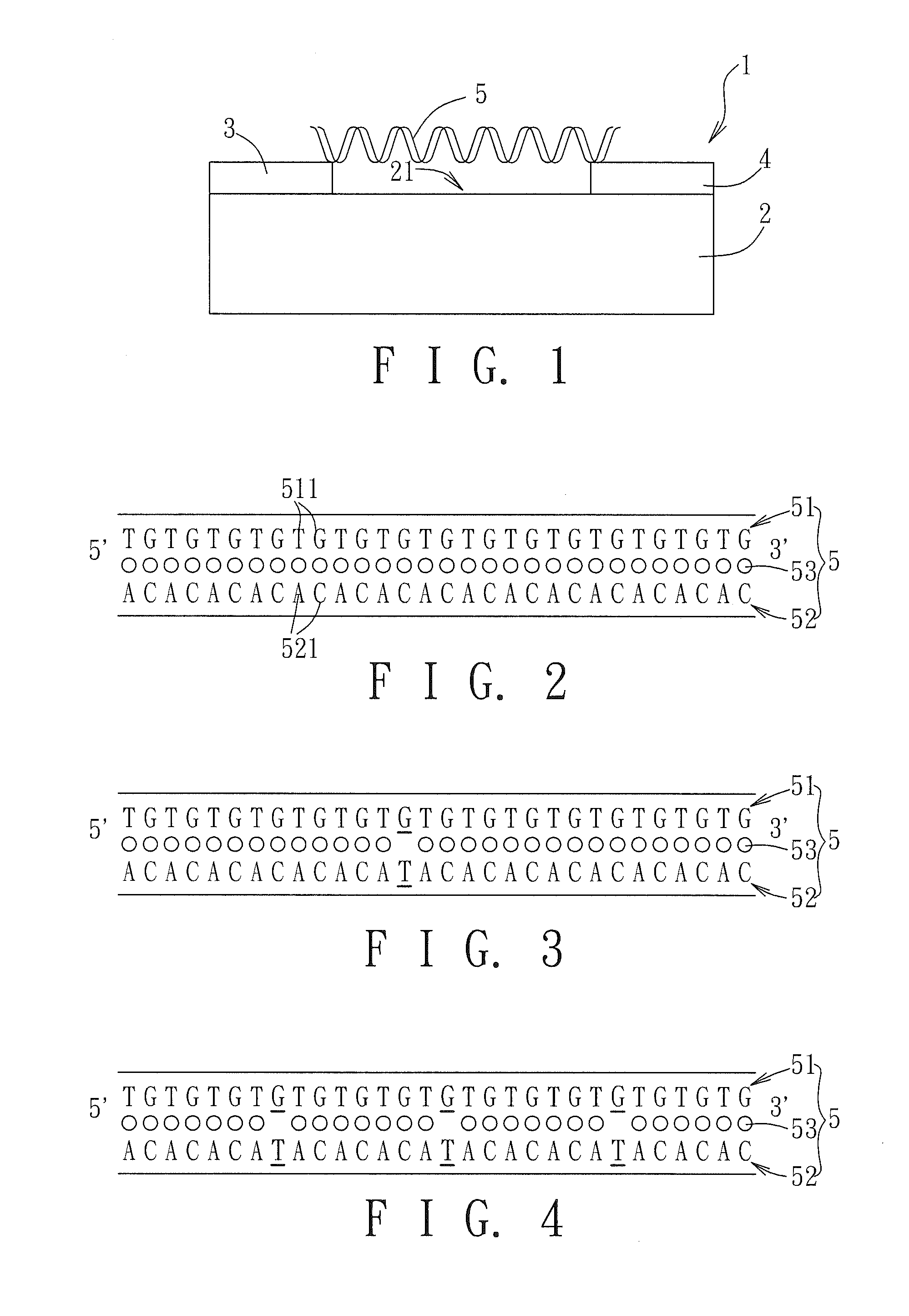
[0042]The bio-nanowire device 1 includes an insulating substrate 2, a first conductor 3, a second conductor 4, and a bio-nanowire 5.

[0043]The substrate 2 has a first surface 21. In this embodiment, the substrate 2 is a silicon substrate th...


PUM


Abstract

A bio-nanowire device includes a substrate having a first surface, a first conductor, a second conductor, and a bio-nanowire. The first and second conductors are disposed on the first surface of the substrate, and are spaced apart from each other. The bio-nanowire has two ends respectively connected to the first and second conductors, and includes a nucleic acid molecule having two nucleotide segments, and a plurality of metal ions bonded between the two nucleotide segments of the nucleic acid molecule. The two nucleotide segments form a double helix structure via base pairs. When a voltage or a current is applied to the bio-nanowire, the oxidation state of the metal ions can be changed such that the non-linear electroconductive characteristic of the bio-nanowire can be controlled.

Description

CROSS-REFERENCE TO RELATED APPLICATION[0001]This application claims priority of Taiwanese Application No. 101134278, filed on Sep. 19, 2012.BACKGROUND OF THE INVENTION[0002]1. Field of the Invention[0003]This invention relates to a nanowire device, more particularly to a bio-nanowire device having the characteristics of non-linear conductors.[0004]2. Description of the Related Art[0005]An ordinary material at a nanoscale exhibits different properties compared to the same material at a macroscopic scale. Currently, numerous semiconductor devices employ nanostructures, such as nanodots, nanowires, nanotubes, etc., so as to improve the properties thereof. For example, Taiwan Patent Publication No. 201218421 proposes a light emitting diode (LED) that uses GaN nanowires, each of which includes a P-type GaN segment and an N-type GaN segment that is connected to the P-type GaN segment. A PN junction is formed at the interface between the aforesaid P-type and N-type GaN segments so that eac...

Claims


Application Information

Patent Timeline
IPC IPC(8): G01N27/02
CPCG01N27/021G01N27/3278
Inventor CHANG, CHIA-CHINGJIAN, WEN-BINCHEN, YU-CHANGYUAN, CHIUN-JYEGU, FRANK
Owner NAT CHIAO TUNG UNIV
Why Eureka
Try Eureka