
Semiconductor device

Active Publication Date: 2014-03-27
RENESAS ELECTRONICS CORP
View PDF4 Cites 1 Cited by
  • Summary
  • Abstract
  • Description
  • Claims
  • Application Information

AI Technical Summary

Benefits of technology

The patent relates to a circuit that generates a reference voltage. The circuit includes a low-voltage transistor. The technical effect of the patent is that it explains how to control the circuit so that the low-voltage transistor is not damaged by the voltage in the sample and hold circuit. This ensures reliable operation of the circuit.

Problems solved by technology

Therefore, when there is a programming error of the user, a problem occurs such that the low-voltage transistor in the reference voltage generating circuit is destroyed.

Method used


Image

  • Semiconductor device
  • Semiconductor device
  • Semiconductor device

Examples


first embodiment

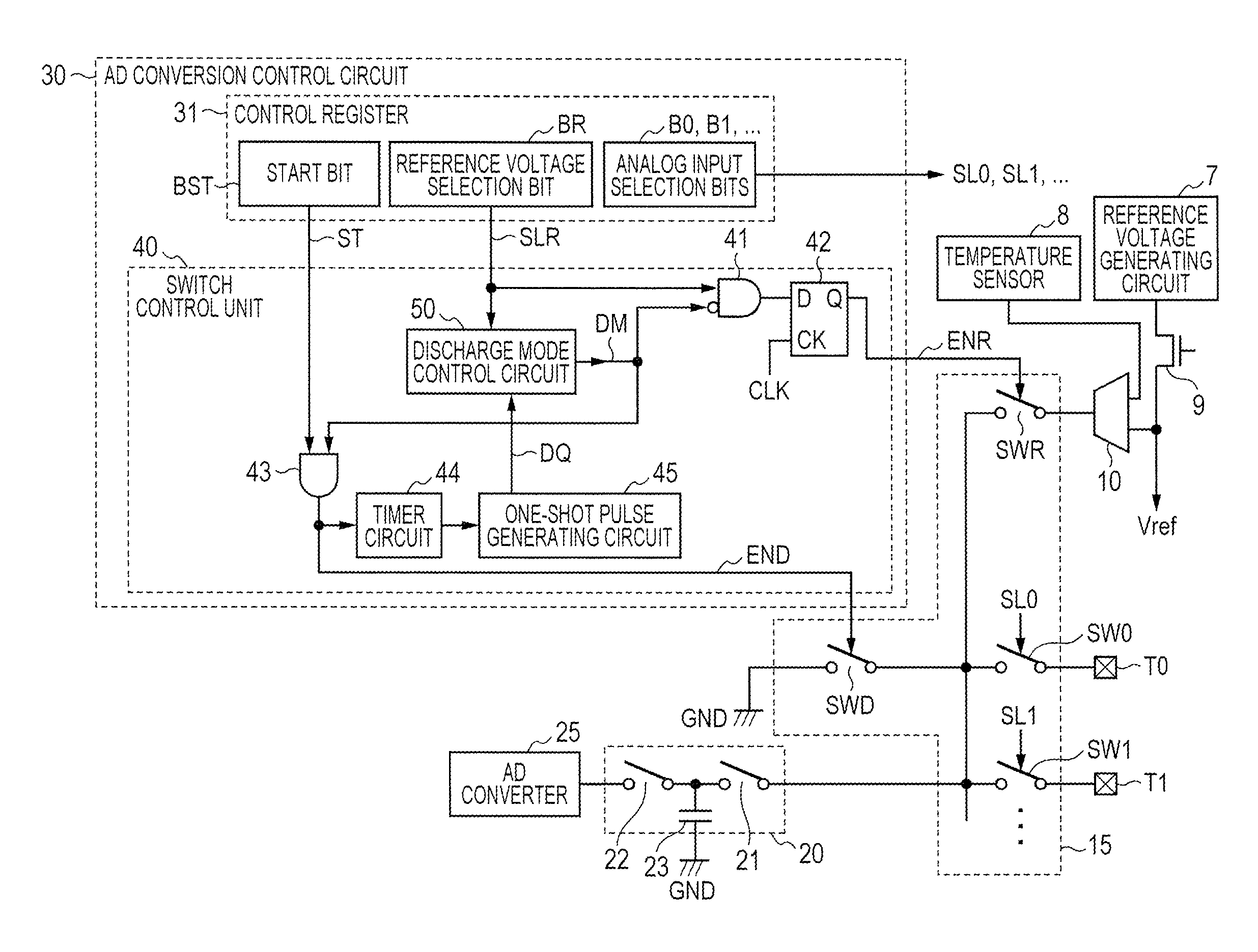
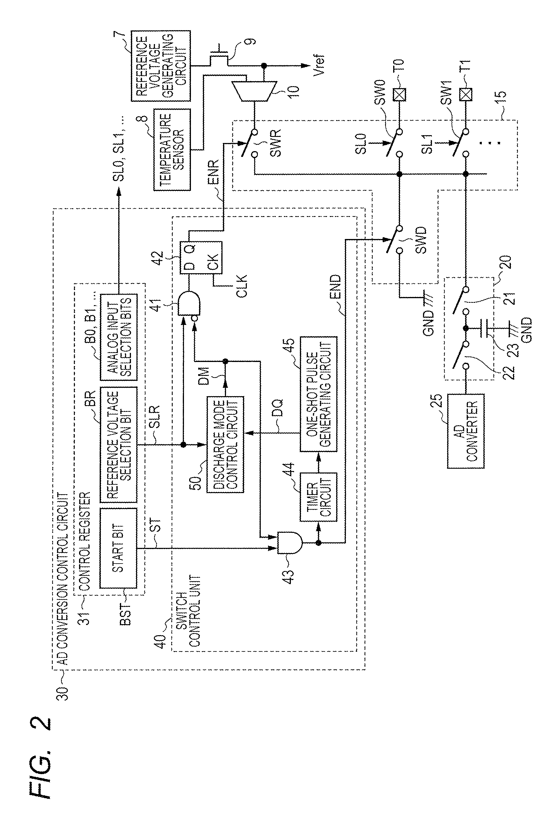
General Configuration of Microcomputer Chip

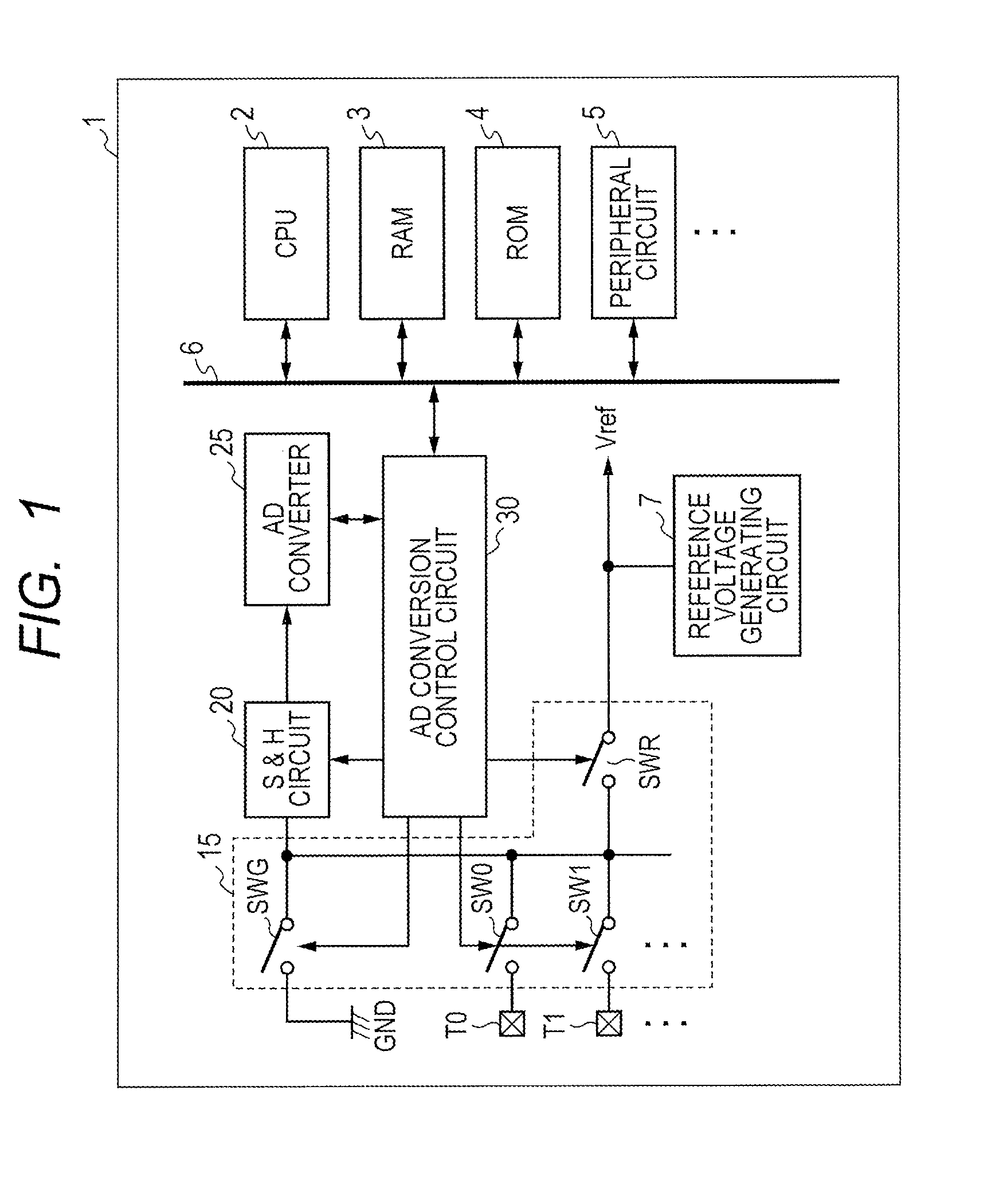
[0023]FIG. 1 is a block diagram illustrating an example of the configuration of a microcomputer chip as a first embodiment.

[0024]Referring to FIG. 1, a microcomputer chip 1 includes a CPU (Central Processing Unit) 2, a RAM (Random. Access Memory) 3, a ROM (Read Only Memory) 4, and other peripheral circuits 5 such as input / output circuits. The components are coupled to one another via a bus 6.

[0025]The CPU 2 controls the general operation of the microcomputer chip 1 by executing a program stored in the RAM 3 and the ROM 4. The RAM 3 and the ROM 4 are used as main storages of the CPU 2.

[0026]The microcomputer chip 1 further includes a sample and hold (S & H) circuit 20, an AD converter 25, an AD conversion control circuit 30, a switching unit 15, and a reference voltage generating circuit 7.

[0027]The AD converter 25 performs AD conversion of voltage held in the sample and hold circuit 20. The AD conversion method may be any of integrating con...

second embodiment

[0062]In the conventional AD conversion control circuit, the user can selectively choose whether the discharge mode is set or not. Specifically, the voltage held in the sample and hold circuit can be discharged not only before execution of the AD conversion of the internal reference voltage or the temperature sensor circuit but also before execution of the AD conversion of analog voltage supplied from the outside. To an AD conversion control circuit of a second embodiment, a function of allowing the user to freely choose whether the voltage held in the sample and hold circuit is discharged or not is added. Hereinafter, it will be concretely described with reference to FIGS. 6 and 7.

[0063]FIG. 6 is a block diagram illustrating the configuration of a part of an AD conversion control circuit as the second embodiment. FIG. 7 is a circuit diagram illustrating the configuration of a discharge mode control circuit in FIG. 6.

[0064]An AD conversion control circuit 30A in FIG. 6 is different ...

third embodiment

[0067]The AD conversion control circuit 30 of the first embodiment is configured to always discharge the voltage held in the sample and hold circuit before performing the AD conversion of the internal reference voltage or the output signal of the temperature sensor circuit. However, in the case where a voltage equal to or less than the withstand voltage of the low-voltage transistor is held in the sample and hold circuit, the low-voltage transistor is not destroyed even if the held voltage is not discharged. Consequently, an AD conversion control circuit 30B of a third embodiment has a configuration to determine whether or not voltage held in the sample and hold circuit is discharged depending on whether or not the voltage held in the sample and hold circuit (that is, the AD conversion result of last time) exceeds the withstand voltage of the low-voltage transistor. Hereinafter, it will be concretely described with reference to FIGS. 8 and 9. The third embodiment can be combined wit...


PUM


Abstract

The present invention realizes reliably control so that, at the time of AD converting reference voltage, a low-voltage transistor in a reference voltage generating circuit is not destroyed by voltage held in a sample and hold circuit. In a semiconductor device, when an instruction of detecting a reference voltage value is received, a switch control unit controlling switching of an input signal of an internal AD converter temporarily automatically couples an input node of a sample and hold circuit and a ground node and, after that, couples the input node of the sample and hold circuit and an output node of a reference voltage generating circuit.

Description

CROSS-REFERENCE TO RELATED APPLICATIONS[0001]The disclosure of Japanese Patent Application No. 2012-212794 filed on Sep. 26, 2012 including the specification, drawings and abstract is incorporated herein by reference in its entirety.BACKGROUND[0002]The present invention relates to a semiconductor device having an AD (Analog-to-Digital) converter.[0003]A semiconductor device (for example, a microcomputer) having therein an AD converter can detect, as digital values, an external input analog voltage, an internal reference voltage value output from a reference voltage generating circuit, an output value of an internal temperature sensor circuit, and the like. The AD converter is used, for example, by a method of monitoring chip environments by periodically AD converting the internal reference voltage value and the output value of the temperature sensor circuit while repeatedly AD converting the external input voltage.[0004]There are also techniques that, in a semiconductor device havin...

Claims


Application Information

Patent Timeline
IPC IPC(8): H03M1/12
CPCH03M1/1245H03M1/06H03M1/12
Inventor MASUDA, TAKAYA
Owner RENESAS ELECTRONICS CORP
Features
  • Generate Ideas
  • Intellectual Property
  • Life Sciences
  • Materials
  • Tech Scout
  • Unparalleled Data Quality
  • Higher Quality Content
  • 60% Fewer Hallucinations
Learn More