

Power switching device and method of manufacturing the same
a technology of power switching device and manufacturing method, which is applied in the direction of semiconductor devices, diodes, electrical apparatus, etc., can solve the problems of high forward turn-on voltage, inability to improve the efficiency of power switching device, and may prove to be a drawback for some applications, so as to reduce reverse leakage current and lower forward turn-on voltage
- Summary
- Abstract
- Description
- Claims
- Application Information
AI Technical Summary
Benefits of technology
Problems solved by technology
Method used
Image

Examples
Embodiment Construction
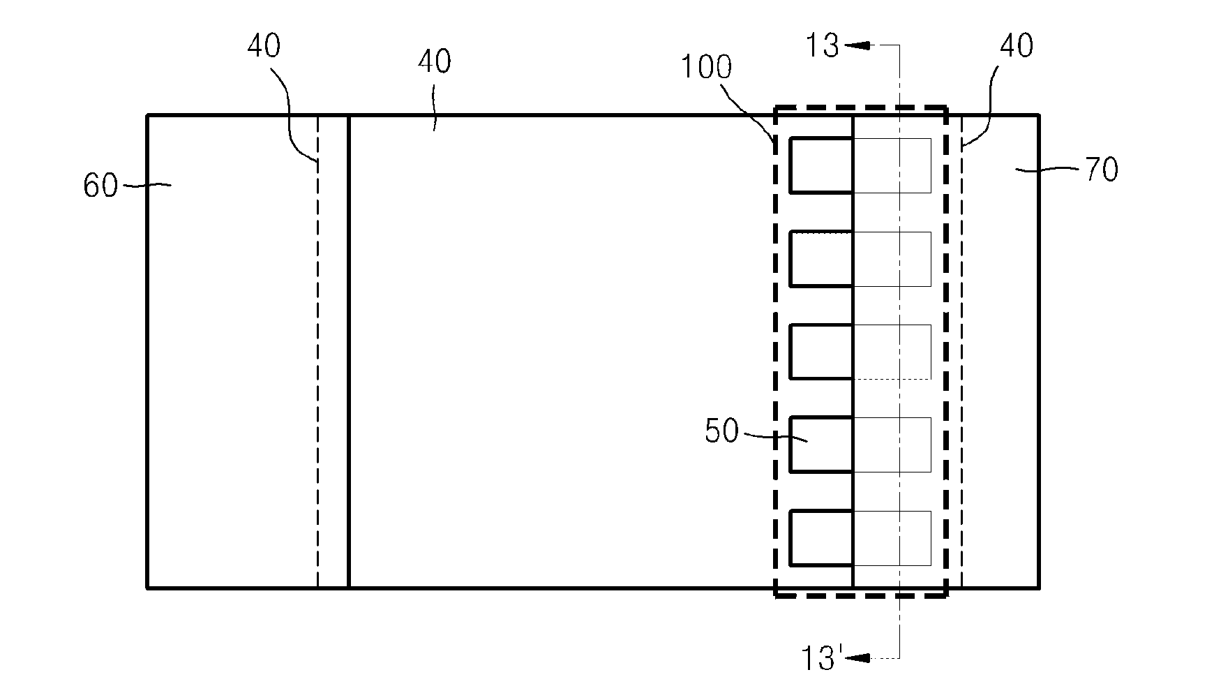
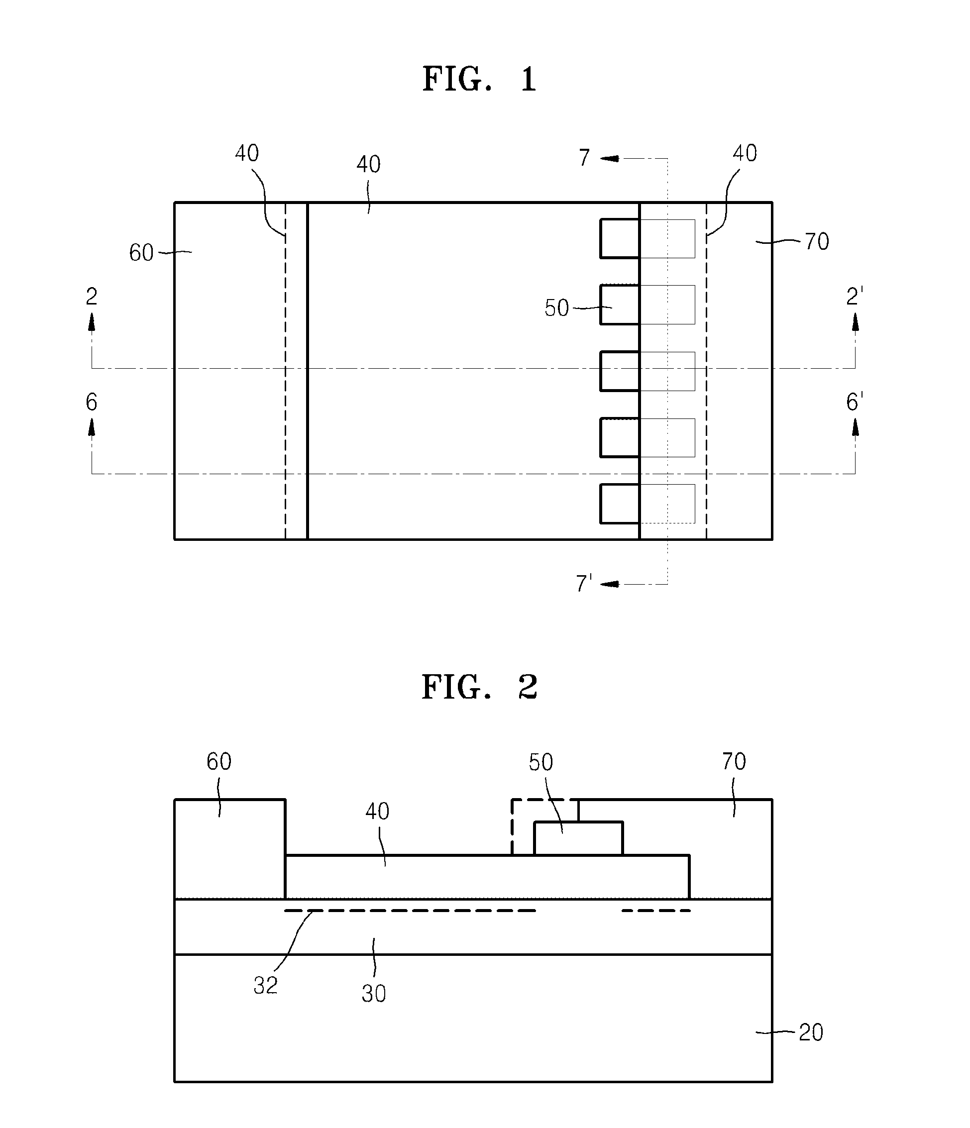
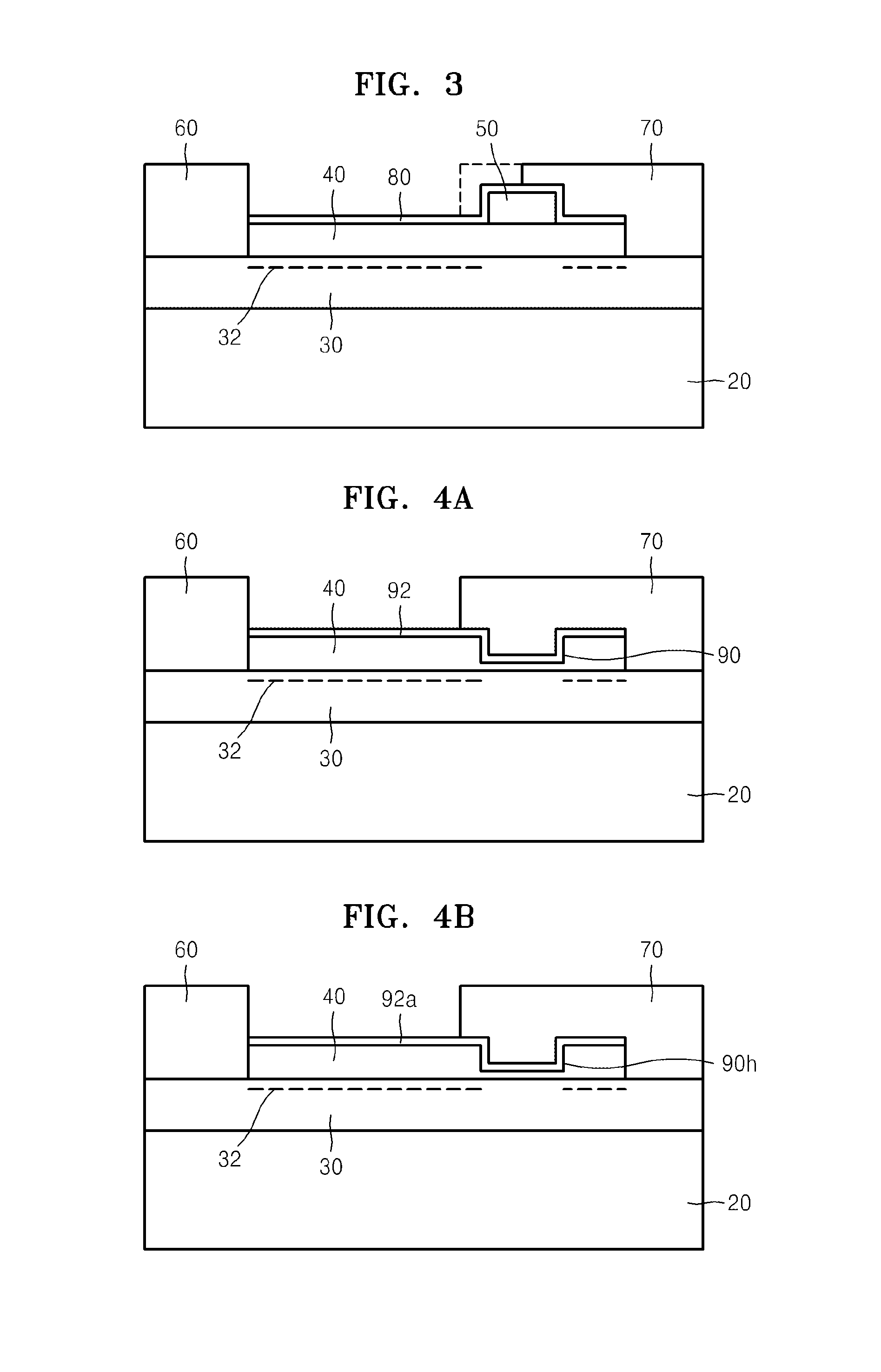
[0038]Detailed example embodiments are disclosed herein. However, specific structural and functional details disclosed herein are merely representative for purposes of describing example embodiments. Example embodiments may, however, be embodied in many alternate forms and should not be construed as limited to only the embodiments set forth herein.
[0039]Accordingly, while example embodiments are capable of various modifications and alternative forms, embodiments thereof are shown by way of example in the drawings and will herein be described in detail. It should be understood, however, that there is no intent to limit example embodiments to the particular forms disclosed, but to the contrary, example embodiments are to cover all modifications, equivalents, and alternatives falling within the scope of example embodiments. Like numbers refer to like elements in the description of the figures.
[0040]It will be understood that, although the ter ms first, second, etc. may be used herein t...
PUM
 Abstract
Description
Claims
Application Information