
Method for Recovering an On-State Forward Voltage and, Shrinking Stacking Faults in Bipolar Semiconductor Devices, and the Bipolar Semiconductor Devices
a technology of stacking faults and forward voltages, applied in semiconductor devices, semiconductor/solid-state device details, instruments, etc., can solve the problems of lowering the properties of elements, various crystal defects, and various crystal defects during the production process
- Summary
- Abstract
- Description
- Claims
- Application Information
AI Technical Summary
Benefits of technology
Problems solved by technology
Method used
Image

Examples
example 1
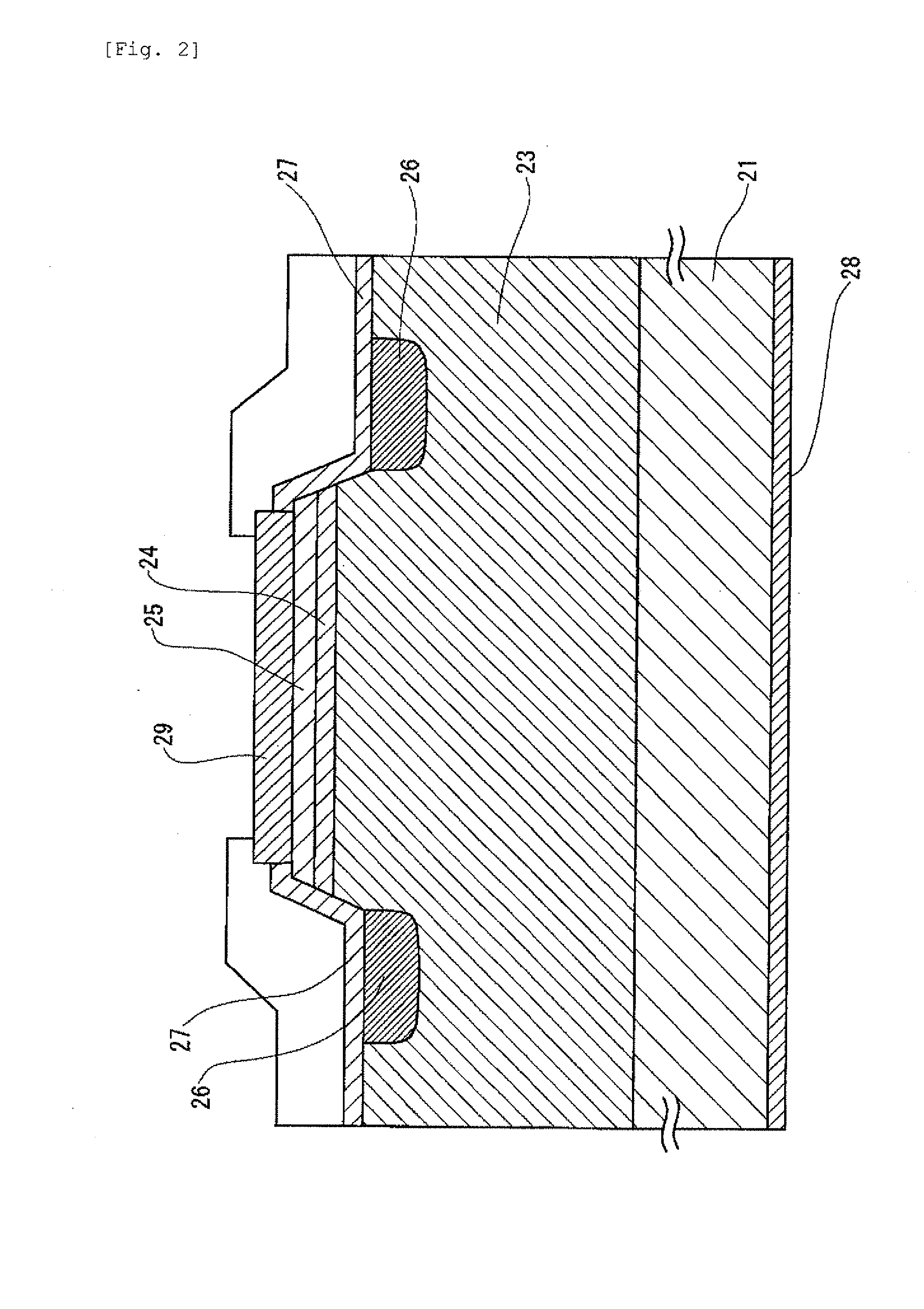
[0118]A pn diode as shown in FIG. 2 was prepared for test. On an n type 4H-SiC (0001) substrate (carrier density of 8×1018 cm−3, 400 μm thick) prepared by slicing an ingot grown by the modified Lely method in an off direction of [11-20] at an off angle of 8° and mirror treating the surface, a nitrogen doped n type SiC layer (donor density of 5×1014 cm−3, 40 μm thick), and an aluminum doped p type SiC layer (p type junction layer: acceptor density of 5×1017 cm−3, 1.5 μm thick and p+ type contact layer: acceptor density of 1×1018 cm−3, 0.5 μm thick) were epitaxially grown in this order.
[0119]Next, the outer peripheral part of the epitaxial film was removed by reacting ion etching (RIE) and a mesa structure having a vertical width of 4 μm was formed. In order to ease the electric field concentration in the mesa bottom, aluminum ions were implanted to the mesa bottom and thereby a JTE having a total dose amount of 1.2×1013 cm−2, a width of 250 μm and a depth of 0.7 μm. After implantatio...
example 2
[0122]Using the pn diode same as prepared in Example 1, an on-state forward bias operation test was carried out in the same conditions as in Example 1. Successively, heating was carried out at 400° C. for 1 hr. Thereafter, the voltage in the forward direction was observed. The results are shown in FIG. 3.
example 3
[0123]Using the pn diode same as prepared in Example 1, an on-state forward bias operation test was carried out in the same conditions as in Example 1. Successively, heating was carried out at 500° C. for 1 hr. Thereafter, the voltage in the forward direction was observed. The results are shown in FIG. 3.
PUM
 Abstract
Description
Claims
Application Information