Method for fabricating flip chip gallium nitride light emitting diode
- Summary
- Abstract
- Description
- Claims
- Application Information
AI Technical Summary
Benefits of technology
Problems solved by technology
Method used
Image
Examples
Embodiment Construction
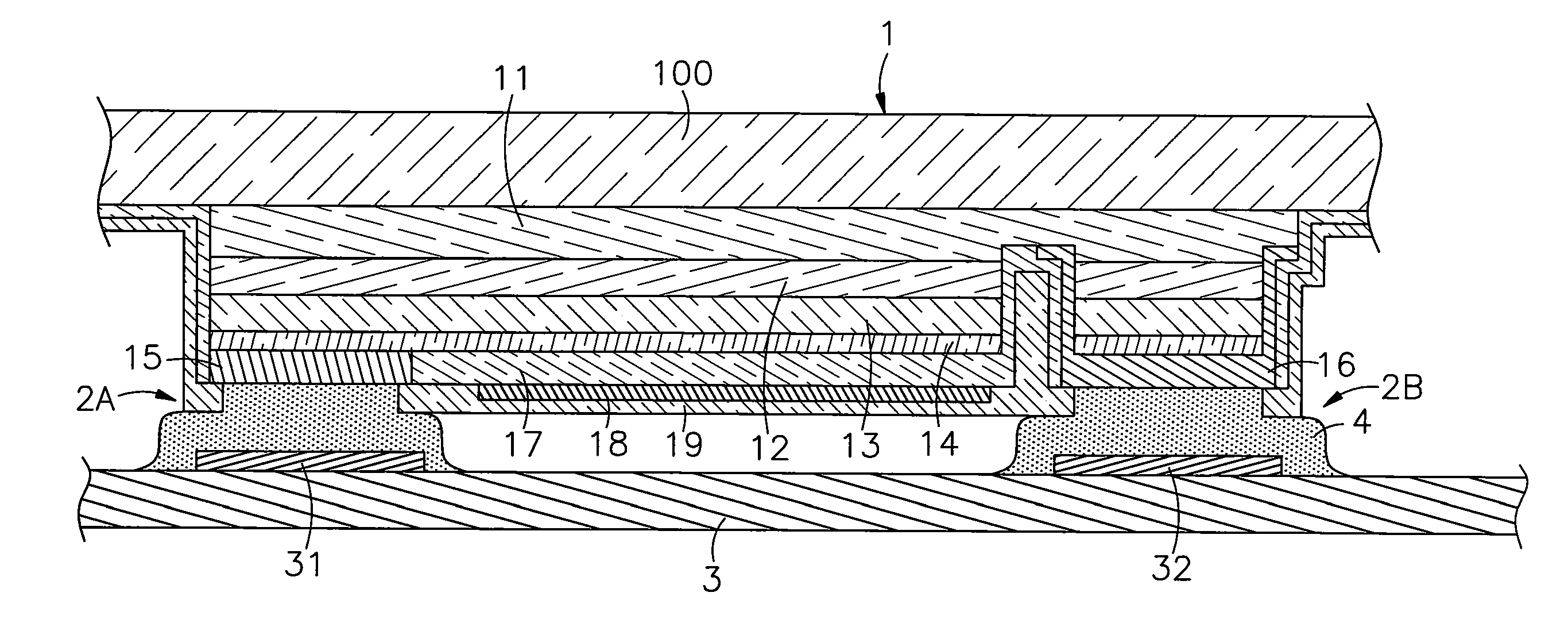
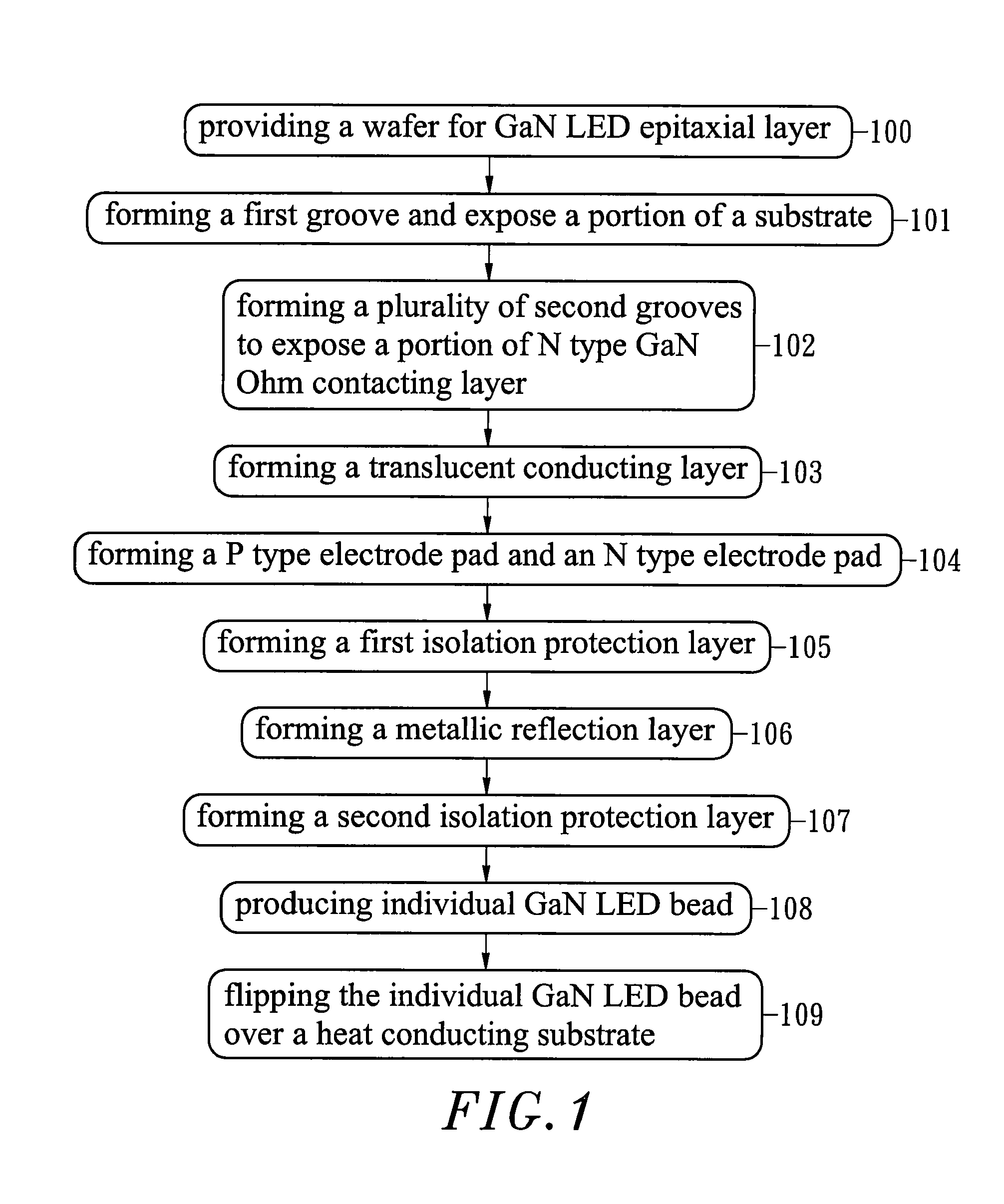
[0033]Referring to FIG. 1, a method for fabricating the flip chip GaN LED bead is described as follows.
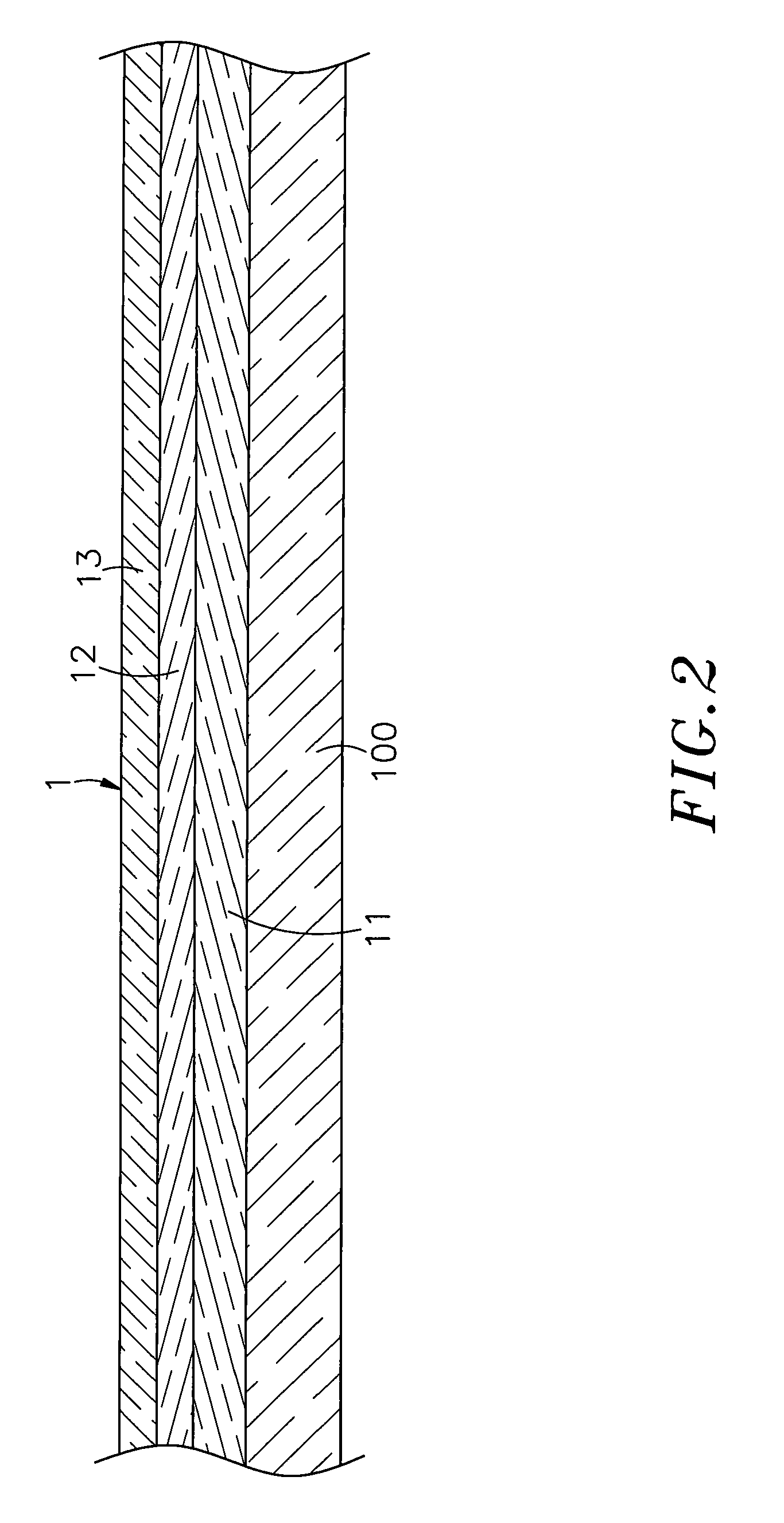
[0034]At step 100, a wafer for GaN LED epitaxial layer 2 is provided.
[0035]At step 101, an etching process is performed to form a first groove 101 and expose a portion of a substrate 100.
[0036]At step 102, an etching process is performed to form a plurality of second grooves 102 adjacent to the first groove 101 and the outer side to respectively form epitaxial layers 2A, 2B on two sides of a N type GaN Ohm contacting layer 11, and the second groove 102.
[0037]At step 103, a translucent conducting layer 14 is formed on a surface of the epitaxial layers 2A, 2B.
[0038]At step 104, a P type electrode pad 15 and an N type electrode pad 16 are formed on a portion of the translucent conducting layer 14.
[0039]At step 105, a first isolation protection layer 17 is formed over the P type electrode pad 15, the N type electrode pad 16, the first groove 101 and the second groove 102.
[0040]At step ...
PUM
 Abstract
Description
Claims
Application Information


