Light-emitting diode, method for making light-emitting diode, integrated light-emitting diode and method for making integrated light-emitting diode, method for growing a nitride-based iii-v group compound semiconductor, light source cell unit, light-emitting diode backlight, and light-emitting diode display and electronic device

a technology of light-emitting diodes and compound semiconductors, which is applied in the field of light-emitting diodes, can solve the problems of difficult to reduce the dislocation density of the gan semiconductor layer and low light-emitting efficiency of the light-emitting diodes, and achieves improved light extraction efficiency, high light-emitting efficiency, and low light-emitting efficiency.

Inactive Publication Date: 2006-11-16
SONY CORP
View PDF14 Cites 70 Cited by
  • Summary
  • Abstract
  • Description
  • Claims
  • Application Information

AI Technical Summary

Benefits of technology

[0013] On the other hand, with another growth method in related art shown in FIGS. 39A to 39F, it is stated that no space is formed between the sapphire substrate 101 and the GaN semiconductor layer 102. However, it is considered difficult to reduce a dislocation density of the GaN semiconductor layer 102 to a level similar to that of the growth method in related art shown in FIGS. 36A to 36C. This leads to the fact that where a light-emitting diode structure is used by growing a GaN semiconductor layer on the GaN semiconductor layer 102 of a high dislocation density, these GaN semiconductor layers also increase in dislocation density, thereby inviting a lowering of light-emitting efficiency.
[0014] It is desirable to provide a light-emitting diode that is remarkably improved in light extraction efficiency by solving the problem on the formation of such a space as discussed above, is significantly improved in crystallinity of a nitride-based III-V group compound semiconductor layer of the light-emitting diode thereby resulting in a very high light-emitting efficiency, and can be manufactured at low costs by one epitaxial growth and also to provide a method for making the diode of a type mentioned above.

Problems solved by technology

According to the test results conducted by the inventors, where a light-emitting diode structure is formed by growing a GaN semiconductor layer on the GaN semiconductor layer 102, there arises a problem in that an emission efficiency of the light-emitting diode is low.
However, it is considered difficult to reduce a dislocation density of the GaN semiconductor layer 102 to a level similar to that of the growth method in related art shown in FIGS. 36A to 36C.

Method used


Image

  • Light-emitting diode, method for making light-emitting diode, integrated light-emitting diode and method for making integrated light-emitting diode, method for growing a nitride-based iii-v group compound semiconductor, light source cell unit, light-emitting diode backlight, and light-emitting diode display and electronic device
  • Light-emitting diode, method for making light-emitting diode, integrated light-emitting diode and method for making integrated light-emitting diode, method for growing a nitride-based iii-v group compound semiconductor, light source cell unit, light-emitting diode backlight, and light-emitting diode display and electronic device
  • Light-emitting diode, method for making light-emitting diode, integrated light-emitting diode and method for making integrated light-emitting diode, method for growing a nitride-based iii-v group compound semiconductor, light source cell unit, light-emitting diode backlight, and light-emitting diode display and electronic device

Examples


first embodiment

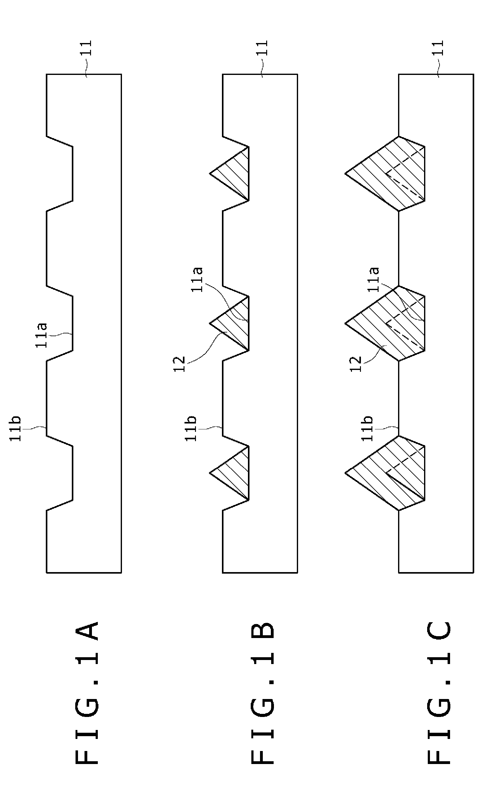
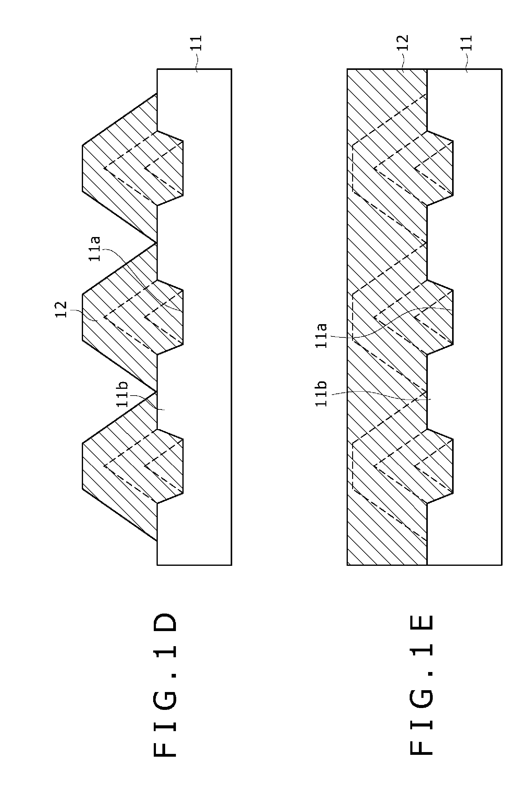
[0104]FIGS. 1A to 1F are views showing, in the order of steps, a method for making a GaN light-emitting diode according to the present invention.

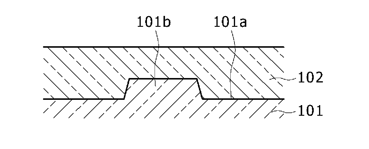
[0105] In this first embodiment, as shown in FIG. 1A, a sapphire substrate 11 having a patterned indentation on one main surface thereof is provided. Reference numeral 11a indicates a recessed portion or recess and reference numeral 11b indicates a protruded portion or protrusion. In this case, the recessed portion 11a has an inverted trapezoid in section. For instance, the main surface of sapphire substrate 11 is a c-face and the recessed portion 11a is in a striped form extending in a direction of the sapphire substrate 11. Although the planar shapes of the recessed portion 11a and the protruded portion 11b may be those ones set out hereinbefore, respectively, preferred instances are shown in FIG. 2. In this instance, as shown in FIG. 2, each of the protruded portions 11b is hexagonal in plane and they are two-dimensionally arranged to b...

fourth embodiment

[0158] the present invention is described.

[0159] In the fourth embodiment, a SiN film 33 is formed, as an amorphous layer, on a flat sapphire substrate 11 over the entire surface thereof, for example, by a vacuum deposition method, a sputtering method, a CVD method or the like in a manner as shown in FIG. 23A. This SiN film 33 has a thickness, for example, of 1 nm or over.

[0160] Next, as shown in FIG. 23B, the sapphire substrate 11 on which the SiN film 33 has been formed is subjected to patterned indentation, for example, by a RIE method, a powder blasting method, a sand blasting method or the like to form recessed portions 11a and protruded portions 11b as in the first embodiment.

[0161] Subsequently, as shown in FIG. 23C, a GaN layer 34 is grown at a low temperature, for example, of about 550° C. The thickness of the GaN layer 34 is, for example, at 200 nm or below. The GaN layer 34 grows separately on the bottom of each recessed portion 11a of sapphire substrate 11 and also on ...


PUM


Abstract

A method for making a light-emitting diode, which including the steps of: providing a substrate having at least one recessed portion on one main surface and growing a first nitride-based III-V group compound semiconductor layer through a state of making a triangle in section having a bottom surface of the recessed portion as a base thereby burying the recessed portion; laterally growing a second nitride-based III-V group compound semiconductor layer from the first nitride-based III-V group compound semiconductor layer over the substrate; and successively growing a third nitride-based III-V group compound semiconductor layer of a first conduction type, an active layer and a fourth nitride-based III-V group compound semiconductor layer of a second conduction type on the second nitride-based III-V group compound semiconductor layer.

Description

CROSS REFERENCES TO RELATED APPLICATIONS [0001] The present invention contains subject matter related to Japanese Patent Application JP 2005-142462 filed in the Japanese Patent Office on May 16, 2005, and Japanese Patent Application JP 2006-105647 filed in the Japanese Patent Office on Apr. 6, 2006, the entire contents both of which are incorporated herein by reference. BACKGROUND OF THE INVENTION [0002] 1. Field of the invention [0003] This invention relates to a light-emitting diode and a method for making same, and also to an integrated light-emitting diode and a method for making same. The present invention also relates to a method for growing a nitride-based III-IV group compound semiconductor, and a light source cell unit, a light-emitting diode backlight, a light-emitting diode display and an electronic device using such a light-emitting diode as mentioned above. More particularly, the present invention relates to a light-emitting diode using a nitride-based III-V group compo...

Claims


Application Information

Patent Timeline
Patent Type & Authority Applications(United States)
IPC IPC(8): H01L21/00H01L33/32H01L33/40H01L33/06H01L33/44H01L33/56H01L33/62
CPCH01L33/007H01L33/12H01L33/22H01L2224/48091H01L2224/48465H01L2924/1305H01L2924/00014H01L2924/00
Inventor OHMAE, AKIRATOMIYA, SHIGETAKAMAEDA, YUKISHIOMI, MICHINORIAMI, TAKAAKIMIYAJIMA, TAKAOYANASHIMA, KATSUNORITANGE, TAKASHIYASUDA, ATSUSHI
Owner SONY CORP
Why Eureka
Try Eureka