Anodizing device, continuous anodizing device, and film forming method

Inactive Publication Date: 2014-04-10
FUJIFILM CORP
View PDF0 Cites 4 Cited by
  • Summary
  • Abstract
  • Description
  • Claims
  • Application Information

AI Technical Summary

Benefits of technology

[0049]Regarding the third object of the present invention, a circulator that moves the electrolytic solution present in a gap between the counter electrode and the web that is supported by the power supply drum in close contact with the web out of the gap is provided. Therefore, the electrolytic solution generating heat along with anodization can be efficiently discharged from the gap. Accordingly, it is possible to form anodic oxide film showing a high degree of film thickness uniformity and having an excellent surface condition. Moreover, it is possible to completely prevent the anodic oxide film from being formed on the side where the power supply drum is in close contact with the web. Consequently, at a stabilized contact resistance, the anodic oxide film showing a high degree of film thickness uniformity and having an excellent surface condition can be formed on one surface of the web.
[0050]Regarding the fourth object of the present invention, a power supplier that is disposed in a position above the liquid surface of the electrolytic solution and applies current to the web is provided. Accordingly, unlike the conventional method of supplying power through the shaft of a drum whose bearing mechanism is complicated, power can be supplied by a simple constitution.
[0051]Since the power supplier is disposed in a position above the liquid surface of the electrolytic solution, the rotating shaft can be placed in a position below the liquid surface of the electrolytic solution, the circumferential surface of the power supply drum can be effectively utilized for producing film, and the production efficiency can be increased.
[0052]Regarding the first to fourth objects, the web is supported by the power supply drum in close contact with the web and directly supplied with power by the power supplier fr

Problems solved by technology

However, the device of JP 6-108289 A is complicated, and the electrolytic solution is diluted with water on the surface of close contact of the drum, so the concentration of the electrolytic solution needs to be continuously managed.
Moreover, there is a possibility that when the water that forms a thin layer on the surface of close contact generates gas by electrolysis, the thin layer may become a gas layer, the contact resistance may increase, and this may lead to sparking.
Therefore, the band easily strays from an end portion of the aluminum foil, and this makes it difficult to perform continuous operation.
Furthermore, there is a possibility that if tension is applied by crimping, the aluminum foil may be wrinkled when it is a thi

Method used


Image

  • Anodizing device, continuous anodizing device, and film forming method
  • Anodizing device, continuous anodizing device, and film forming method
  • Anodizing device, continuous anodizing device, and film forming method

Examples


Embodiment Construction

[0084]Hereinafter, the anodizing device, the continuous anodizing device, and the film forming method of the present invention will be described in detail by using drawings.

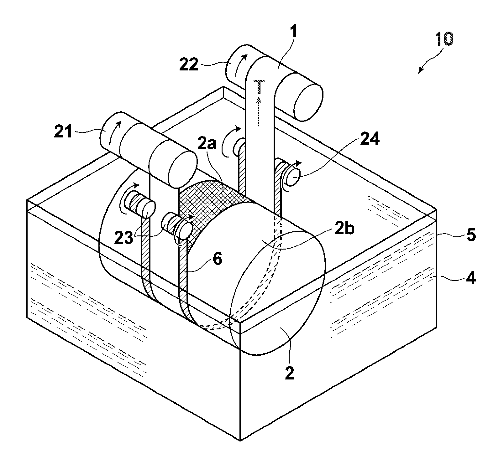
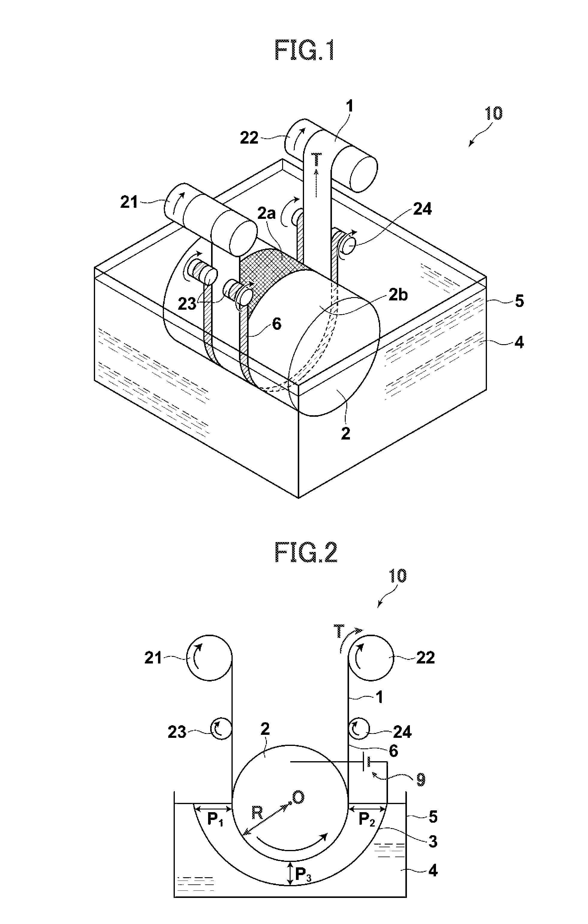
[0085]FIG. 1 is a schematic perspective view showing an anodizing device of an embodiment for achieving a first object of the present invention, and FIG. 2 is a schematic cross-sectional view of the anodizing device of the embodiment for achieving the first object that is shown in FIG. 1.

[0086]Hereinafter, the anodizing device used in common for achieving the first to fourth objects of the present invention will be described.

[0087]As shown in FIGS. 1 and 2, an anodizing device 10 of the present invention has a power supply drum 2 which is in close contact with and supports a web made of an anodizable metal or a web 1 made of composite conductive metal foil of which at least one surface is composed of an anodizable metal (hereinafter, also called simply “web 1”), and in which at least a portion 2a that is in close...


PUM

PropertyMeasurementUnit
Currentaaaaaaaaaa
Electrical conductoraaaaaaaaaa
Electric potential / voltageaaaaaaaaaa

Abstract

An anodizing device has: a power supply drum that supports, in close contact therewith, a web consisting of an anodizable metal and has a part configured with a conductive material, to which the web is closely attached; a counter electrode provided facing the power supply drum; an electrolysis tank filled with an electrolyte, into which part of the power supply drum and the counter electrode are immersed; a protection member formed of a non-conductive material that protects the lateral direction end portions of the web supported by the power supply drum in close contact therewith and a portion of the power supply drum, to which the web is not closely attached, from the electrolyte; and a driver adapted to make the web and the protection member travel concurrently in the electrolyte in synchronization with the circumferential speed of the power supply drum.

Description

BACKGROUND OF THE INVENTION[0001]The present invention relates to an anodizing device, a continuous anodizing device, and a film forming method suitable for producing substrates for semiconductor elements that are usefully utilized in semiconductor devices such as solar cells, thin-film transistor circuits, and displays (image display devices), and electrodes for electrolytic condensers.[0002]Thin-film solar cells using a substrate made of a metal have a possibility of being used for various purposes compared to those using a glass substrate, in view of the lightness and flexibility of the substrate. Moreover, since the substrate made of a metal can endure a high-temperature process, photoelectric conversion characteristics are improved, and accordingly, a highly efficient solar cell can be expected.[0003]In a solar cell module, solar cells are integrated by being connected to one another in series on the same substrate, thereby improving the module efficiency. At this time, an insu...

Claims


Application Information

Patent Timeline
IPC IPC(8): C25D11/04C25D7/06
CPCC25D7/0614C25D11/04C25D11/022C25D11/005C25D11/045
Inventor YUYA, SHIGENORISATO, KEIGOKAITO, RYOZO
Owner FUJIFILM CORP
Why Eureka
Try Eureka