Semiconductor device having a self-forming barrier layer at via bottom

a technology of barrier layer and silicon-based semiconductor, which is applied in the field of silicon-based semiconductor devices, can solve the problems of adverse effects on the reliability of the device, the device being subject to high temperatures,

a technology of barrier layer and silicon-based semiconductor, which is applied in the field of silicon-based semiconductor devices, can solve the problems of adverse effects on the reliability of the device, the device being subject to high temperatures,

US20140097538A1Active Publication Date: 2014-04-10GLOBALFOUNDRIES US INC

Image

  • Semiconductor device having a self-forming barrier layer at via bottom
  • Semiconductor device having a self-forming barrier layer at via bottom
  • Semiconductor device having a self-forming barrier layer at via bottom

Examples


Embodiment Construction

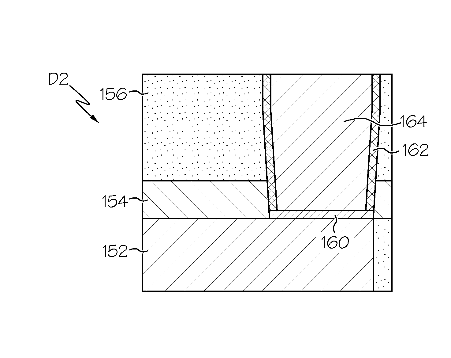
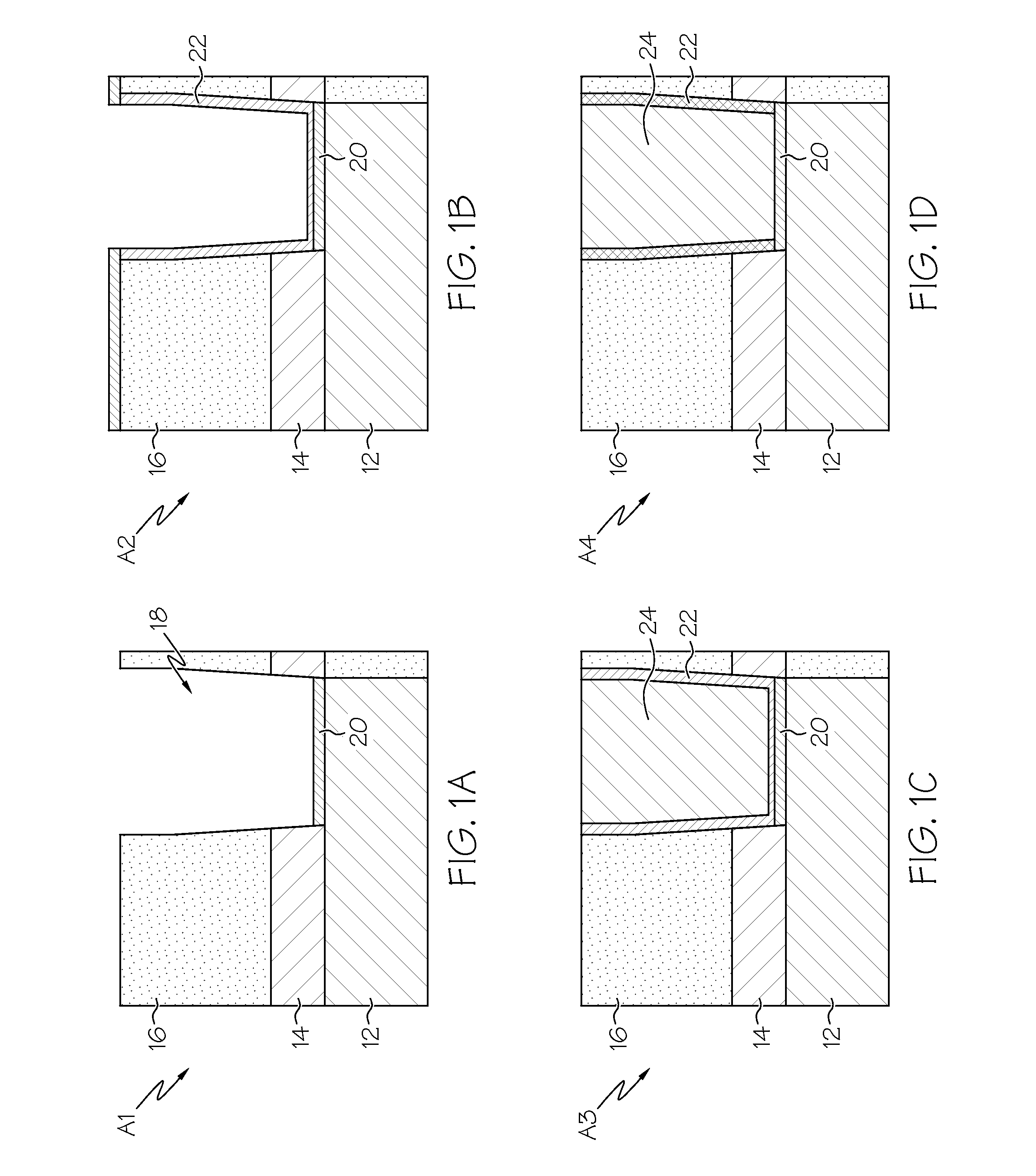
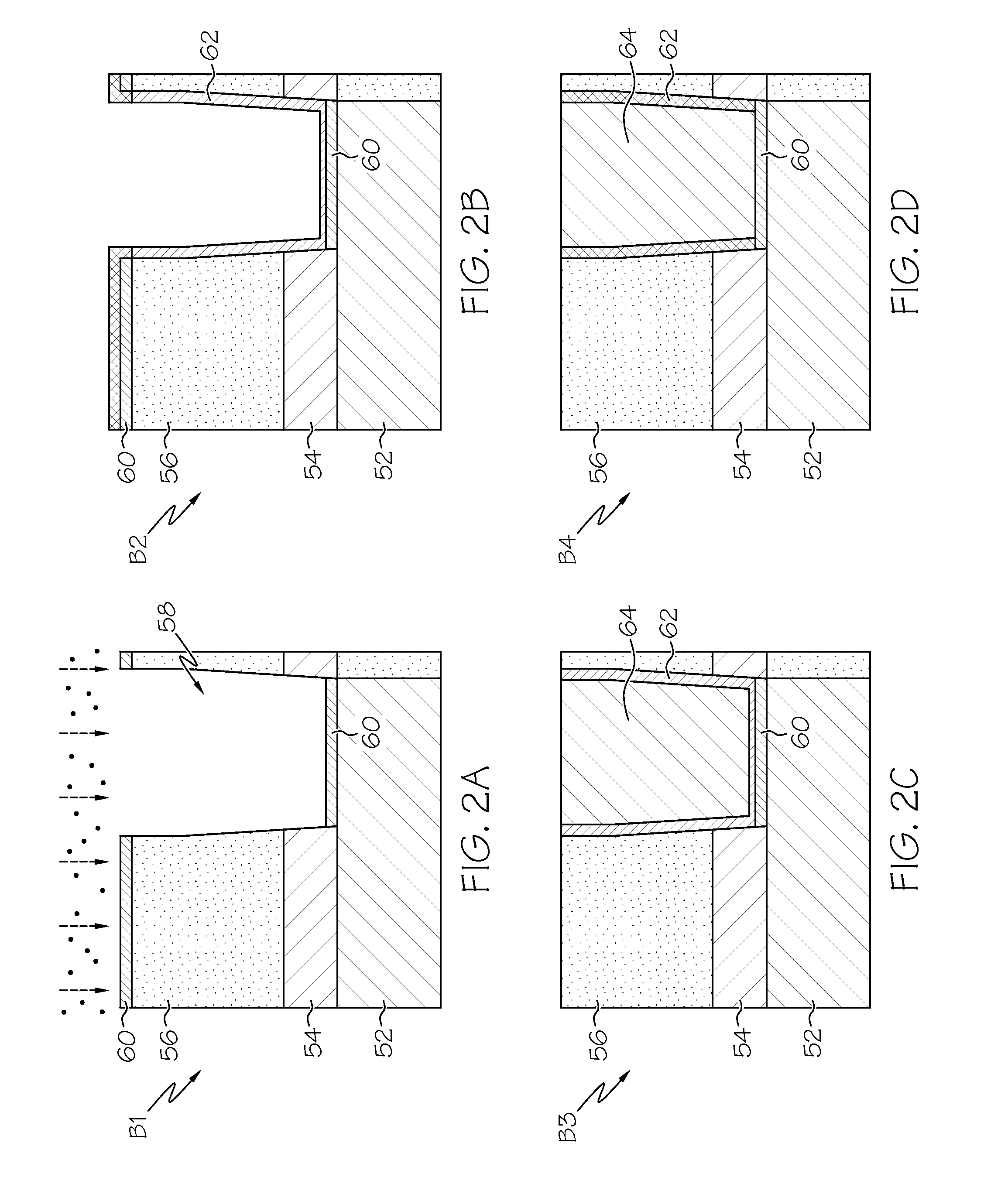
[0017]Illustrative embodiments will now be described more fully herein with reference to the accompanying drawings, in which embodiments are shown. This disclosure may, however, be embodied in many different forms and should not be construed as limited to the embodiments set forth herein. Rather, these embodiments are provided so that this disclosure will be thorough and complete and will fully convey the scope of this disclosure to those skilled in the art. In the description, details of well-known features and techniques may be omitted to avoid unnecessarily obscuring the presented embodiments.

[0018]The terminology used herein is for the purpose of describing particular embodiments only and is not intended to be limiting of this disclosure. As used herein, the singular forms β€œa”, β€œan”, and β€œthe” are intended to include the plural forms as well, unless the context clearly indicates otherwise. Furthermore, the use of the terms β€œa”, β€œan”, etc., do not denote a limitation of quantity,...


PUM


Abstract

An approach for forming a semiconductor device is provided. In general, the device is formed by providing a metal layer, a cap layer over the metal layer, and an ultra low k layer over the cap layer. A via is then formed through the ultra low k layer and the cap layer. Once the via is formed, a barrier layer (e.g., cobalt (Co), tantalum (Ta), cobalt-tungsten-phosphide (CoWP), or other metal capable of acting as a copper (CU) diffusion barrier) is selectively applied to a bottom surface of the via. A liner layer (e.g., manganese (MN) or aluminum (AL)) is then applied to a set of sidewalls of the via. The via may then be filled with a subsequent metal layer (with or without a seed layer), and the device may the then be further processed (e.g., annealed).

Description

BACKGROUND[0001]1. Technical Field[0002]This invention relates generally to the field of semiconductors and, more particularly, to approaches for applying a self-forming barrier layer along bottom surfaces of vias, trenches, or the like.[0003]2. Related Art[0004]The semiconductor integrated circuit (IC) industry has experienced rapid growth in recent years. Specifically, generations of ICs have been produced whereby each generation has smaller and more complex circuits than the previous generation. However, for these advances to be realized, developments in IC processing and manufacturing are needed. Under this course of IC evolution, functional density (i.e., the number of interconnected devices per chip area) has generally increased while geometry size (i.e., the smallest component that can be created using a fabrication process) has decreased.[0005]Semiconductor devices are typically formed using multiple layers of material, including conductive, semi-conductive, dielectric, and ...

Claims


Application Information

Patent Timeline
10 Apr 2014
Publication
US20140097538A1
IPC
H01L21/768; H01L23/48
CPC
H01L21/76831; H01L21/76846; H01L21/76855; H01L23/5226; H01L23/53238; H01L23/53295; H01L2924/0002; H01L2924/00
Inventors
ZHAO, LARRY; HE, MING