Thin film transistor and fabricating method

Active Publication Date: 2014-04-10
NAT APPLIED RES LAB
View PDF9 Cites 0 Cited by
  • Summary
  • Abstract
  • Description
  • Claims
  • Application Information

AI Technical Summary

Benefits of technology

The present invention is a method to create a nanascale CMOS device that can be smaller, use less photomasks, and have less complicated gate structure processes affecting its element characteristics. Additionally, this device has a gate that can be easily covered evenly by a gate dielectric layer. This method involves a thin-film transistor with a semiconductor panel, dielectric layer, semiconductor film layer, conduct layer, source, and drain.

Problems solved by technology

However, how to fabricate nanoscale CMOS devices and parasitic resistances effect are problems.
However, the electronic device has a device size that is hard to make smaller.
However, the vertical FET structure requires six photomasks to be fabricated.
However, the nonvolatile memory device requires an extra hard mask to form an insulating device nanowire.
The side-gate is difficult to cover with a gate dielectric layer.

Method used


Image

  • Thin film transistor and fabricating method
  • Thin film transistor and fabricating method
  • Thin film transistor and fabricating method

Examples


Embodiment Construction

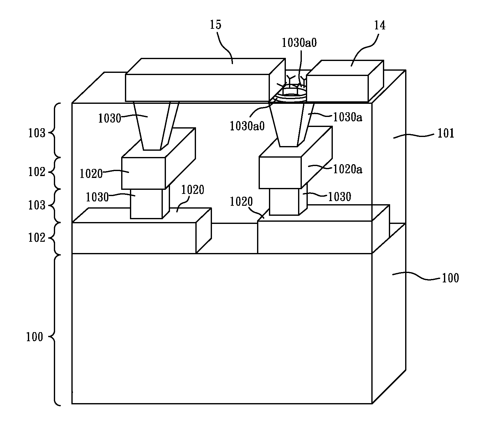
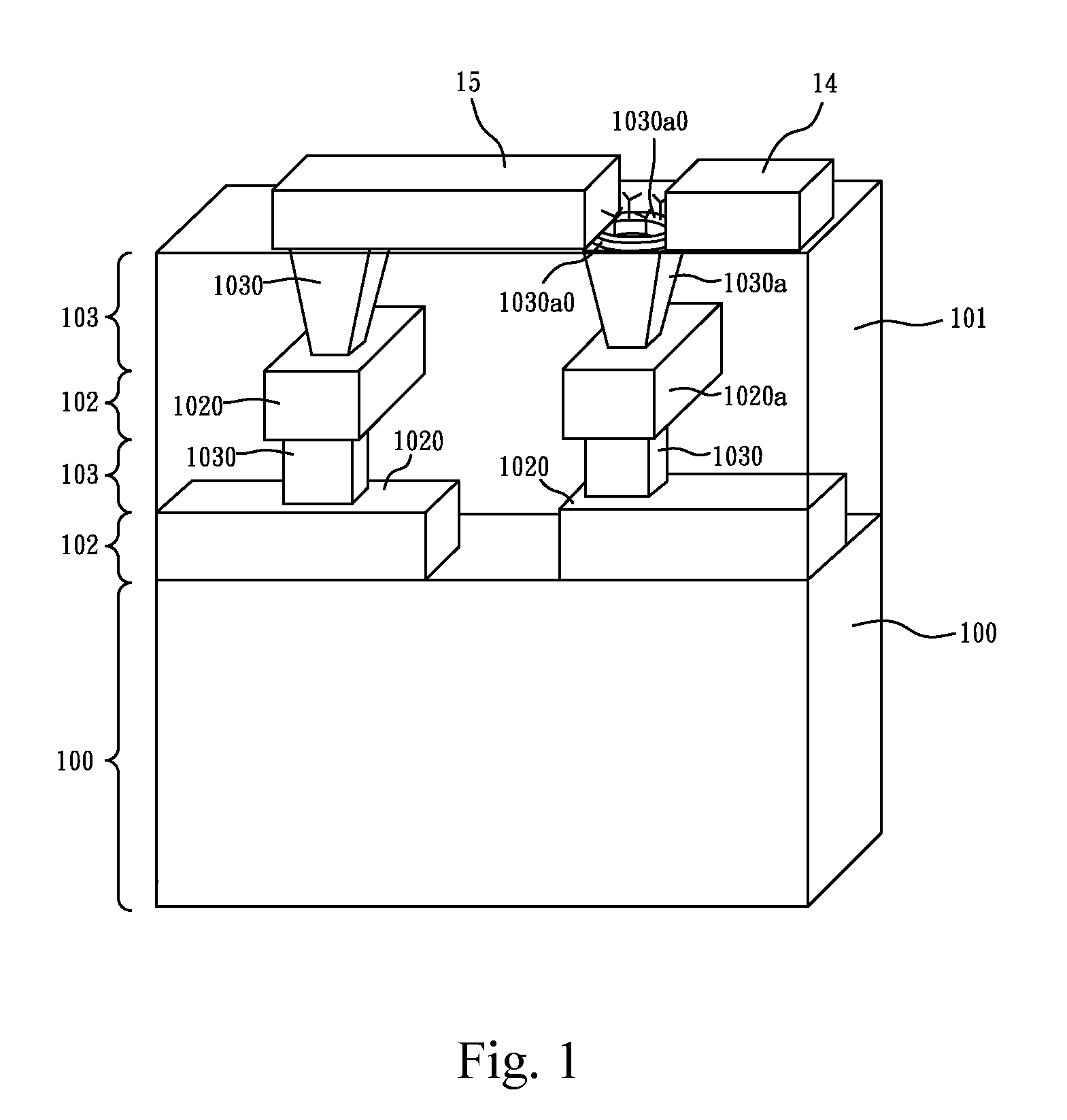
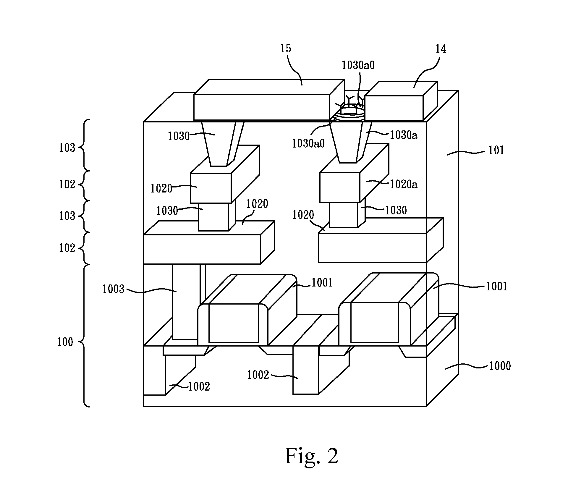
[0035]With reference to FIGS. 1 and 6a to 6h, a thin-film transistor (1) in accordance with the present invention can reduce its device size, decrease photomasks needed, has an element characteristic that is not significantly affected by a complicated gate structure process, has a gate that is easy to be covered evenly by a gate dielectric layer and comprises a semiconductor panel (10), a dielectric layer (11), a semiconductor film layer (12), a conduct layer (13), a source (14) and a drain (15) and may have a threshold voltage. The semiconductor panel (10) comprises a base (100), an intra-dielectric layer (101), at least one metal wire layer (102) and at least one via layer (103).

[0036]With further reference to FIG. 2, the base (100) may comprise at least one complementary metal-oxide-semiconductor well (1000), at least one poly-silicon thin film transistor (1001), at least one shallow trench isolation unit (1002) and at least one contact channel (1003). The poly-silicon thin film ...


PUM


Abstract

A thin-film transistor comprises a semiconductor panel, a dielectric layer, a semiconductor film layer, a conduct layer, a source and a drain. The semiconductor panel comprises a base, an intra-dielectric layer, at least one metal wire layer and at least one via layer. The dielectric layer is stacked on the semiconductor panel. The semiconductor film layer is stacked on the dielectric layer. The conduct layer is formed on the semiconductor film layer. The source is formed on the via of the vias that is adjacent to and connects to the gate via. The drain is formed on another via of the vias that is adjacent to and connects to the gate via. A fabricating method for a thin-film transistor with metal-gates and nano-wires is also disclosed.

Description

CROSS-REFERENCE TO RELATED APPLICATION[0001]This application is a continuation-in-part (CIP) of an U.S. application with application Ser. No. 13 / 451,390, filed on Apr. 19, 2012, which further claims priority from application No. 100147632, filed on Dec. 21, 2011 in the Taiwan Intellectual Property Office.FIELD OF THE INVENTION[0002]The present invention is a thin film transistor and fabricating method.BACKGROUND OF THE INVENTION[0003]Recently, single-chips have been developed using a complementary metal-oxide-semiconductor (CMOS) process and has been applied in an element array. To increase density of the element array, the CMOS process needs to be reduced by using nanoscale CMOS devices. However, how to fabricate nanoscale CMOS devices and parasitic resistances effect are problems.[0004]U.S. Patent No. 2005 / 0176226 A1 discloses a method of manufacturing an electronic device comprising a bottom-gate TFT. The method comprises steps of: forming a doped amorphous silicon gate layer on ...

Claims


Application Information

Patent Timeline
IPC IPC(8): H01L27/12H01L21/84
CPCH01L21/84H01L27/127B82Y10/00H01L21/8238H01L27/092H01L27/1203H01L29/0676H01L27/0688H01L29/0665
Inventor CHEN, MIN-CHENGLIN, CHANG-HSIENLIN, CHIA-YILAI, TUNG-YENHO, CHIA-HUA
Owner NAT APPLIED RES LAB
Why Eureka
Try Eureka