
Package substrate and method of fabricating the same

a technology of packaging substrate and substrate, which is applied in the direction of printed circuit manufacturing, semiconductor/solid-state device details, printed element electric connection formation, etc., can solve the problem that the packaging substrate cannot be applied to modern chips and electronic products

Active Publication Date: 2014-04-17
IND TECH RES INST +1
View PDF7 Cites 27 Cited by
  • Summary
  • Abstract
  • Description
  • Claims
  • Application Information

AI Technical Summary

Benefits of technology

The present patent text provides a package substrate and a method for fabricating it. The package substrate includes an interposer with a redistribution layer and conductive through via, a photo-sensitive dielectric layer, and conductive via. The method involves forming the pattern of the conductive through via and redistribution layer on the interposer, then adding the photo-sensitive dielectric layer on top, followed by the formation of a via for the conductive through via and a conductive via connected to it. This invention allows for the efficient and reliable fabrication of package substrates.

Problems solved by technology

Such a package substrate cannot be applied to the modern chips and electronic products.

Method used


Image

  • Package substrate and method of fabricating the same
  • Package substrate and method of fabricating the same
  • Package substrate and method of fabricating the same

Examples


Embodiment Construction

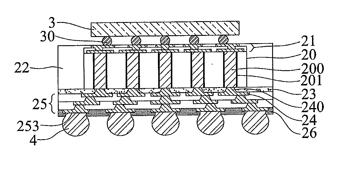
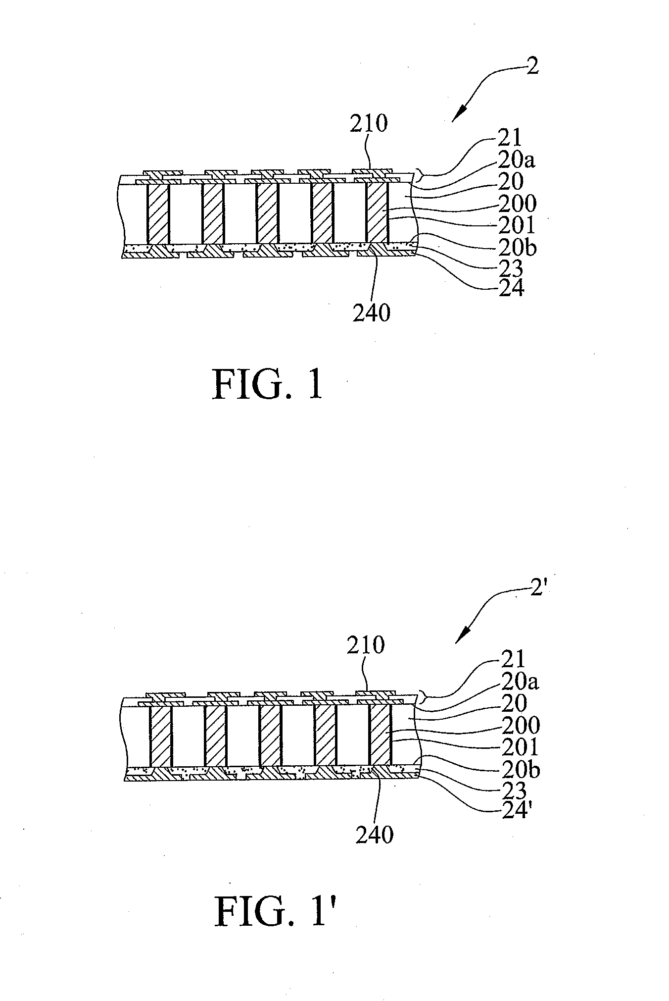
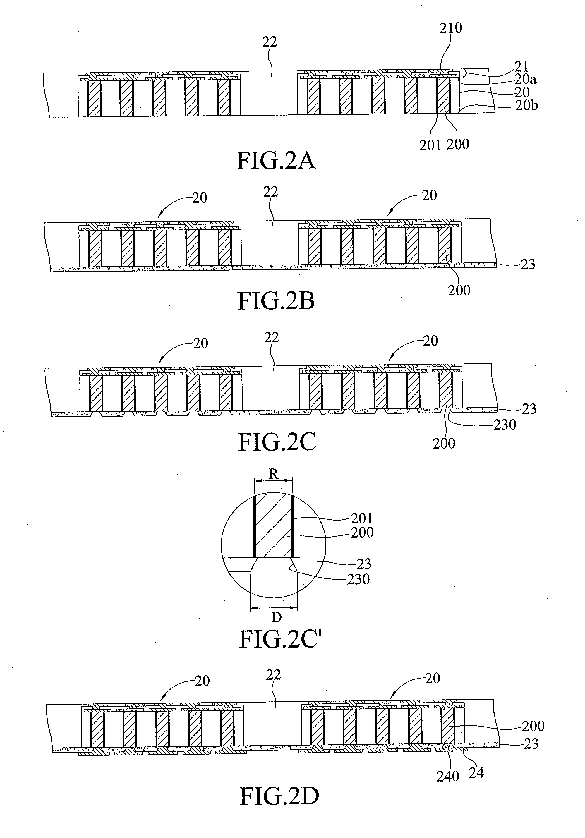
[0015]In the following detailed description, for purposes of explanation, numerous specific details are set forth in order to provide a through understanding of the disclosed embodiments. It will be apparent, however, that one or more embodiments may be practiced without these specific details. In other instances, well-known structures and devices are schematically shown in order to simplify the drawing.

[0016]It should be noted that the structures, proportions, sizes and the like shown in the attached drawings are to be considered only in conjunction with the contents of this specification to facilitate understanding and reading of those skilled in the art, and are not intended to limit the scope of present disclosure, thus they do not hold any real technically significance, and any changes or modifications in the structures, the proportions, the sizes and the like should fall within the scope of the technical contents disclosed in the present disclosure as long as they do not affec...


PUM

PropertyMeasurementUnit
end-surface diameteraaaaaaaaaa
diameteraaaaaaaaaa
diameteraaaaaaaaaa

Abstract

A package substrate and a method of fabricating the package substrate are provided. The package substrate may include an interposer having at least one conductive through via, a photo-sensitive dielectric layer formed on one side of the interposer, and at least one conductive via formed in the photo-sensitive dielectric layer and electrically connected to the conductive through via. By means of a photo lithography process with high alignment accuracy, at least one via with an extremely small diameter can be formed on the photo-sensitive dielectric layer and align with the conductive through via. Therefore, the conductive through via can have its diameter reduced as required, without considering the alignment with the at least one via. Accordingly, the interconnection density of the conductive through via on the interposer is increased.

Description

CROSS-REFERENCE TO RELATED APPLICATIONS[0001]This application claims priority to Taiwanese Patent Application No. 101137406, filed on Oct. 11, 2012.BACKGROUND[0002]1. Technical Field[0003]The present disclosure relates to package substrates, and, relating to a package substrate having an interposer embedded therein and a method of fabricating the package substrate.[0004]2. Description of Related Art[0005]With the growing demands for low-profiled and compact-sized electronic products, a chip has to have a great layout density, and the pitches of contacts on the chip are dramatically reduced accordingly (e.g., a few nanometers). The conductive contacts of a flip-chip package substrate have pitches as great as a few micrometers. Such a package substrate cannot be applied to the modern chips and electronic products.[0006]In order to solve the above-mentioned problems, a silicon interposer is added between the package substrate and the semiconductor chip, metal is electroplated in the si...

Claims


Application Information

Patent Timeline
Patent Type & Authority Applications(United States)
IPC IPC(8): H05K3/40H05K1/11
CPCH05K1/115H05K3/4038H01L2224/16225H01L2924/15311H01L23/147H01L23/49816H01L23/49822H01L23/49827Y10T29/49165
Inventor CHEN, YU-HUALO, WEI-CHUNGHU, DYI-CHUNGHSIEH, CHANG-HONG
Owner IND TECH RES INST
Learn More