Field effect transistor having phase transition material incorporated into one or more components for reduced leakage current

a field effect transistor and phase transition material technology, applied in the direction of semiconductor devices, basic electric elements, electrical appliances, etc., can solve problems such as reducing circuit speed, and achieve the effects of minimizing gidl, minimizing leakage current, and minimizing leakage curren

Active Publication Date: 2014-04-24
GLOBALFOUNDRIES US INC
View PDF5 Cites 36 Cited by
  • Summary
  • Abstract
  • Description
  • Claims
  • Application Information

AI Technical Summary

Problems solved by technology

However, both solutions tend to lower drive current, thereby result in reduced circuit speed when the MOSFET is in the ON state.

Method used


Image

  • Field effect transistor having phase transition material incorporated into one or more components for reduced leakage current
  • Field effect transistor having phase transition material incorporated into one or more components for reduced leakage current
  • Field effect transistor having phase transition material incorporated into one or more components for reduced leakage current

Examples


Embodiment Construction

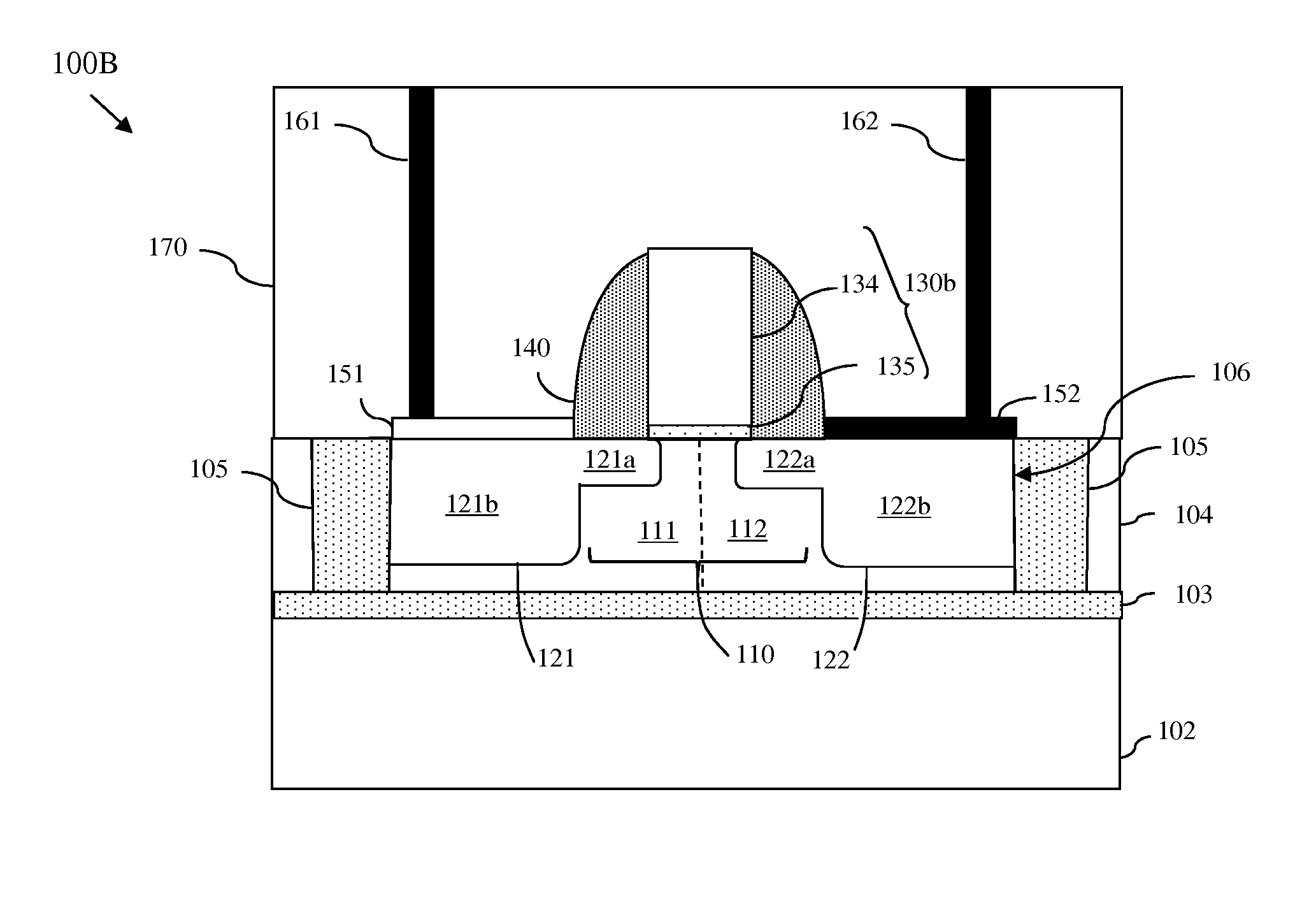
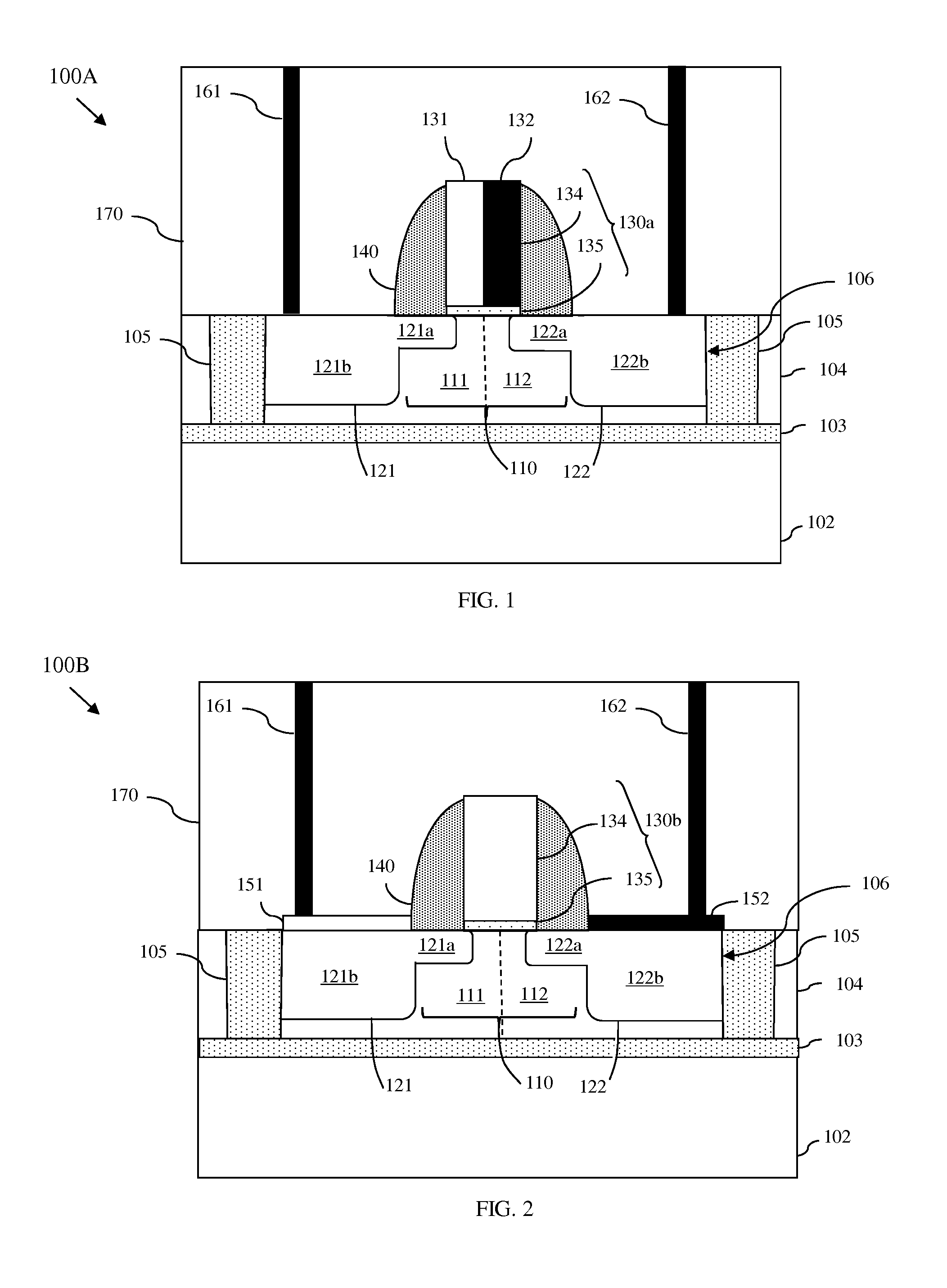
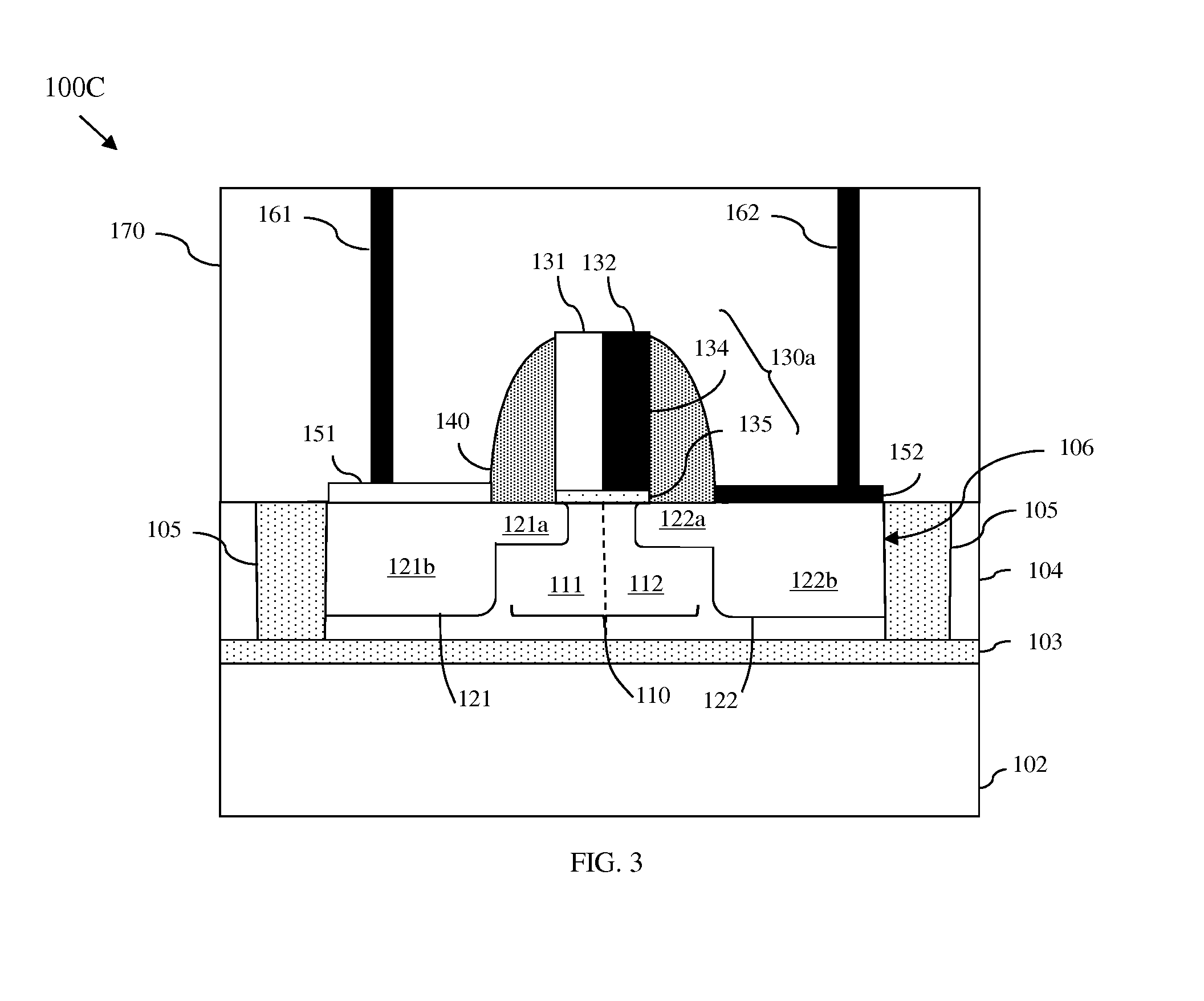
[0031]As discussed above, with metal oxide semiconductor field effect transistors (MOSFETs), Gate-Induced Drain Leakage (GIDL) often places a lower bound on leakage and / or gate dielectric thickness for low-power designs. GIDL refers to the high electric field and, particularly, the band-to-band tunneling that occurs at the channel region to drain region interface overlapped by the gate structure, when the MOSFET is in an OFF state and when the drain region is close to the power-supply voltage such that the voltage difference between the drain region and the source region (VDS) is relatively high. To minimize GIDL, MOSFETs are often designed such that the gate structure does not or only minimally overlaps the interface and / or with a relatively thick gate dielectric layer. However, both solutions tend to lower drive current, thereby result in reduced circuit speed when the MOSFET is in the ON state.

[0032]In view of the foregoing, disclosed herein are embodiments of a metal oxide semic...


PUM


Abstract

Disclosed is a metal oxide semiconductor field effect transistor (MOSFET) having phase transition material incorporated into one or more components and an associated method. The MOSFET can comprise an asymmetric gate electrode having a phase transition material section (e.g., a chromium or titanium-doped vanadium dioxide (VO2) section) above the drain-side of the channel region. Additionally or alternatively, the MOSFET can comprise source and drain contact landing pads comprising different phase transition materials (e.g., un-doped VO2 and chromium or titanium-doped VO2, respectively). In any case, the phase transition material(s) are pre-selected so as to be insulative when the MOSFET is in the OFF state and the voltage difference between the drain region and the source region (VDS) is high in order to minimize leakage current and so as to be conductive when the MOSFET is in the ON state and VDS is high in order to maintain drive current.

Description

BACKGROUND[0001]1. Field of the Invention[0002]The embodiments disclosed herein are related to metal oxide semiconductor field effect transistors (MOSFETs) and, more particularly, to a MOSFET structure having phase transition material incorporated into one or more components in order to minimize leakage current, such as Gate-Induced Drain Leakage (GIDL), when the MOSFET is in its OFF state.[0003]2. Description of the Related Art[0004]In metal oxide semiconductor field effect transistors (MOSFETs), Gate-Induced Drain Leakage (GIDL) often places a lower bound on leakage and / or gate dielectric thickness for low-power designs. GIDL refers to the high electric field and, particularly, the band-to-hand tunneling that occurs at the channel region to drain region interface overlapped by the gate structure, when the MOSFET is in an OFF state and when the drain region is close to the power-supply voltage such that the voltage difference between the drain region and the source region (VDS) is ...

Claims


Application Information

Patent Timeline
Patent Type & Authority Applications(United States)
IPC IPC(8): H01L29/78H01L21/336
CPCH01L21/28088H01L29/4966H01L29/4983H01L29/66545H01L29/7833
Inventor MURALI, KOTA V. R. M.NOWAK, EDWARD J.PARKIN, STUART P.
Owner GLOBALFOUNDRIES US INC
Why Eureka
Try Eureka