Wire bondable surface for microelectronic devices

Active Publication Date: 2014-04-24
ATOTECH DEUT GMBH
View PDF5 Cites 1 Cited by
  • Summary
  • Abstract
  • Description
  • Claims
  • Application Information

AI Technical Summary

Benefits of technology

The present invention provides a metal and metal alloy layer sequence with a wire bondable surface that reduces the risk of bridging and protects sensitive regions of a microelectronic device during wire bonding. This is achieved by using a thinner barrier layer, which provides both enough mechanical stability and prevents damage to sensitive areas.

Problems solved by technology

At the same time the risk of bridging, i.e. an undesired electrical contact between contact areas is increasing.
However, at the same time the mechanical protection of sensitive regions beneath the contact area during wire bonding is not sufficient anymore and device failures caused by wire bonding are observed.

Method used


Image

  • Wire bondable surface for microelectronic devices
  • Wire bondable surface for microelectronic devices

Examples


example 2

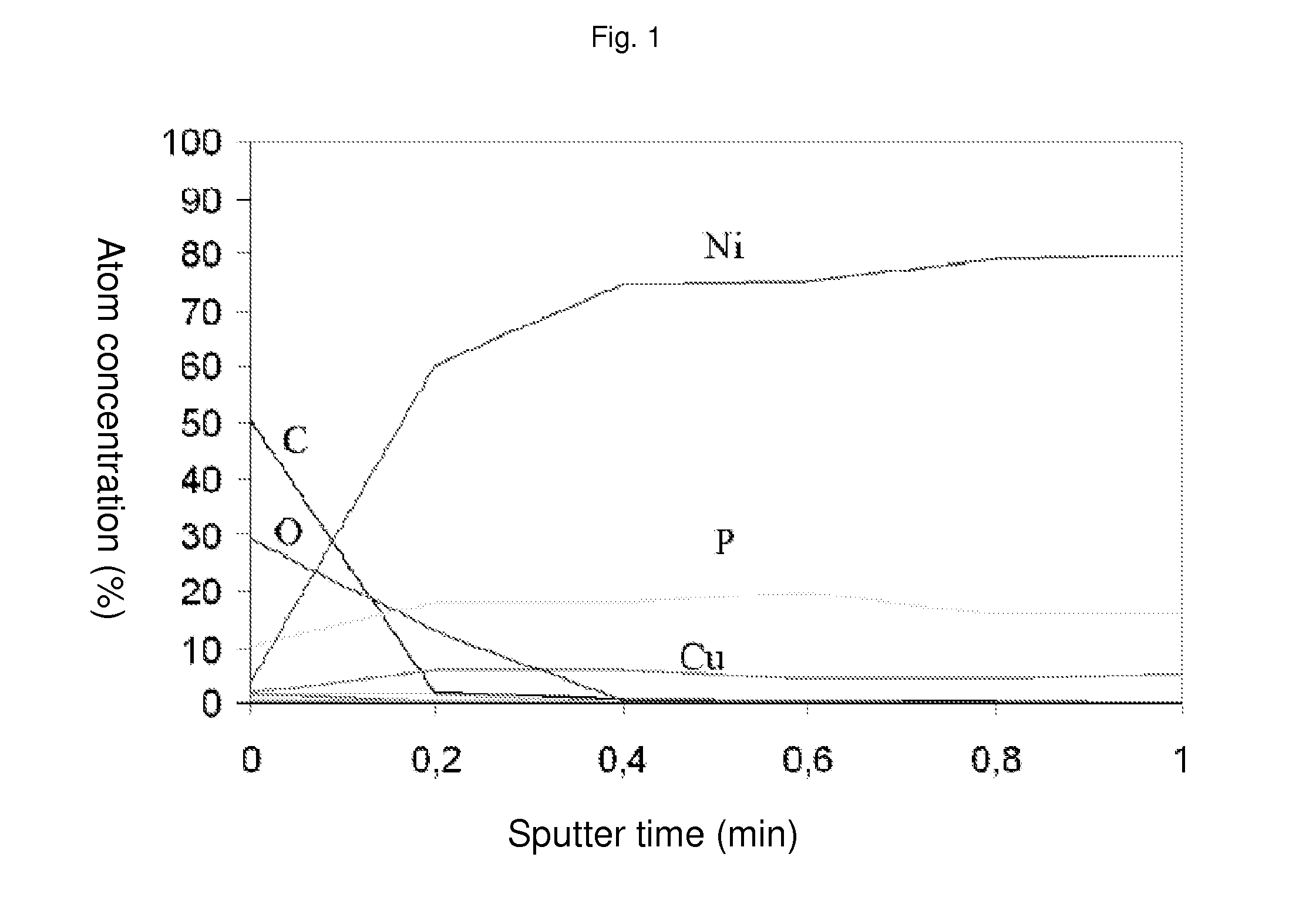
[0055]A Co—W—P alloy was deposited by electroplating onto contact pads made of copper. The thickness of said Co—W—P alloy was 0.2 μm and the phosphorous concentration was 3 wt.-% after deposition.

[0056]Thermal annealing and XPS measurement were performed as described in Example 1.

[0057]A negligible amount of copper was detected in the Co—W—P alloy layer after thermal annealing.

[0058]Hence, a thin Co—W—P alloy layer does prevent copper diffusion at an elevated temperature.

example 3

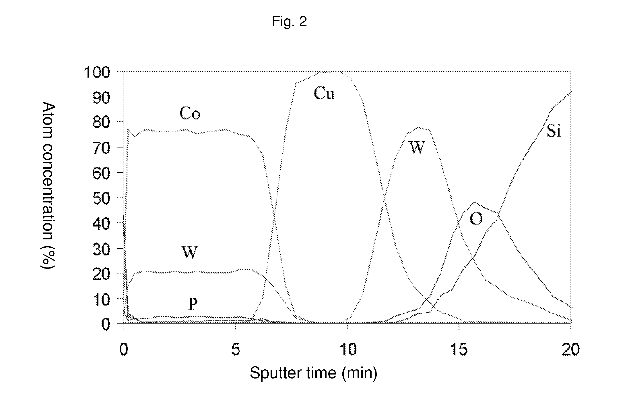
[0059]A Co—W—P alloy was deposited by electroplating onto contact pads made of copper. The thickness of said Co—W—P alloy was 0.2 μm and the phosphorous concentration was 3 wt.-% after deposition.

[0060]Next, an intermediate layer of pure palladium (thickness: 0.3 μm) and thereafter a top layer of gold (thickness: 0.03 μm) was deposited onto the palladium layer.

[0061]The wire bonding properties of the final metal and metal alloy layer sequence consisting of a copper contact pad, a Co—W—P alloy layer, a palladium layer having a palladium content of more than 99 wt.-% and a gold layer were determined using the DVS Standard No 2811.

[0062]A TS bonder model Delvotec 5410 and a gold wires Au-AH3 (Hereaus) and bonding parameters US power 75% (graduation marks (not calibrated marks), specific parameter for given TS bonder); 25 gf bonding force and 25 ms bonding time were used. Measurements were done for 30 stud bumps per pad size.

[0063]The following parameters were determined during the bond...


PUM


Abstract

The present invention concerns thin diffusion barriers in metal and metal alloy layer sequences of contact area / barrier layer / first bonding layer type for metal wire bonding applications. The diffusion barrier is selected from Co-M-P. Co-M-B and Co-M-B—P alloys wherein M is selected from Mn, Zr, Re, Mo, Ta and W having a thickness in the range 0.03 to 0.3 μm. The first bonding layer is selected from palladium and palladium alloys.

Description

FIELD OF THE INVENTION[0001]The present invention relates to metal and metal alloy layer sequences on semi-conducting substrates for metal wire bonding applications.BACKGROUND OF THE INVENTION[0002]Microelectronic devices made of semiconducting substrates such as silicon wafers comprise contact areas on the outer surface which are utilized to provide electrical contacts between the microelectronic device and an IC substrate or a printed circuit board. Such contact areas which can be either in the form of contact pads or bump structures usually consist of copper, copper alloys, aluminium or aluminium alloys. In order to provide such an electrical contact soldering and wire bonding are applied.[0003]In both cases the contact areas must be prepared to provide solderability and bondability by depositing metal or metal alloy layers on top of the contact areas which provide functionalities of a barrier layer and a first and / or second bondable surface.[0004]The barrier layer prevents diffu...

Claims


Application Information

Patent Timeline
IPC IPC(8): H01L23/482
CPCH01L23/4827H01L24/03H01L24/05H01L2224/05124H01L2224/05147H01L2224/05157H01L2224/05164H01L2224/05644H01L2224/05664H01L2924/01013H01L2924/01025H01L2924/01029H01L2924/0103H01L2924/01033H01L2924/01051H01L2924/01061H01L2924/01073H01L2924/01079H01L2924/01082H01L2924/014H01L2924/01005H01L2924/01006H01L2924/01019H01L2924/01024H01L2924/0104H01L2924/01042H01L2924/0105H01L2924/01074H01L2924/01075H01L2224/45144H01L2224/45147H01L2924/10253H01L2924/00014H01L2924/01015H01L23/485
Inventor UHLIG, ALBRECHTGAIDA, JOSEFSUCHENTRUNK, CHRISTOF
Owner ATOTECH DEUT GMBH
Why Eureka
Try Eureka