This helps you quickly interpret patents by identifying the three key elements:
Problems solved by technology
Method used
Benefits of technology
Benefits of technology
The patent aims to make semiconductor devices more tolerant to electrostatic discharge (ESD) by designing a circuit that can handle surge currents better. This results in a uniform operation of the circuit components, which increases the overall ESD tolerance of the semiconductor device.
Problems solved by technology
A surge current caused by ESD is, however, an extremely large and instantaneous current.
Consequently it is significantly difficult to define the layout of the NMOS transistor based on the surge current.
In contrast, it is practically almost impossible to quantify the dependency of the ESD tolerance on the layout of the NMOS transistor, either.
Method used
Image
Click on the blue label to locate the original text in one second.
Reading with bidirectional positioning of images and text.
Examples
first embodiment
[0017]Now, the present invention is described with reference to the accompanying drawings.
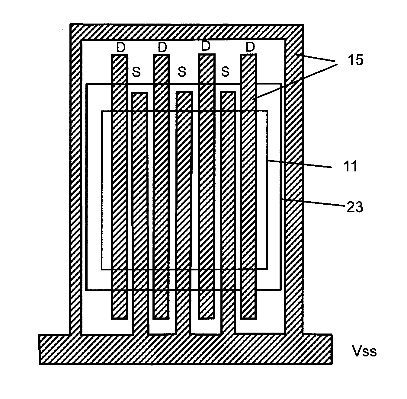
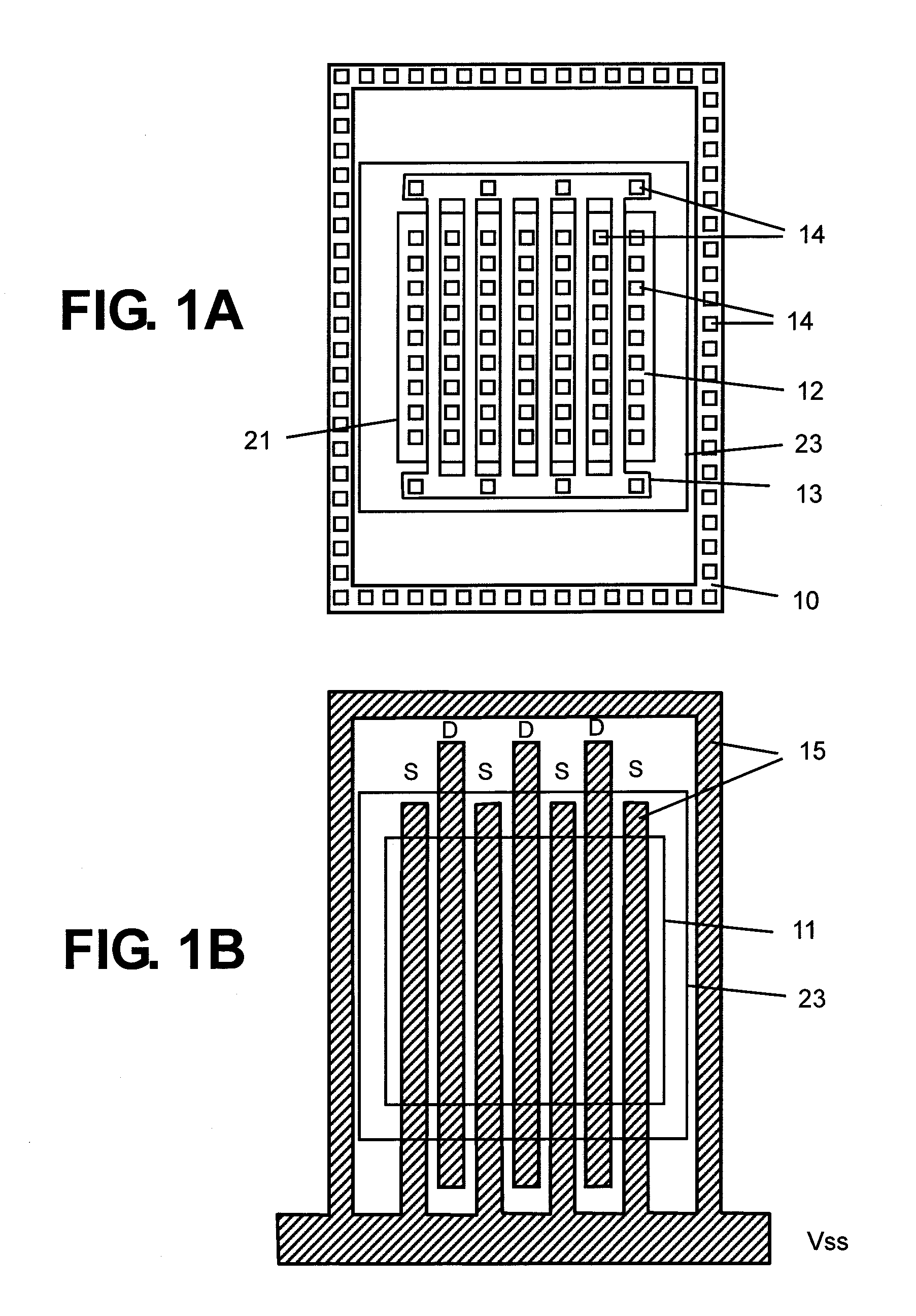
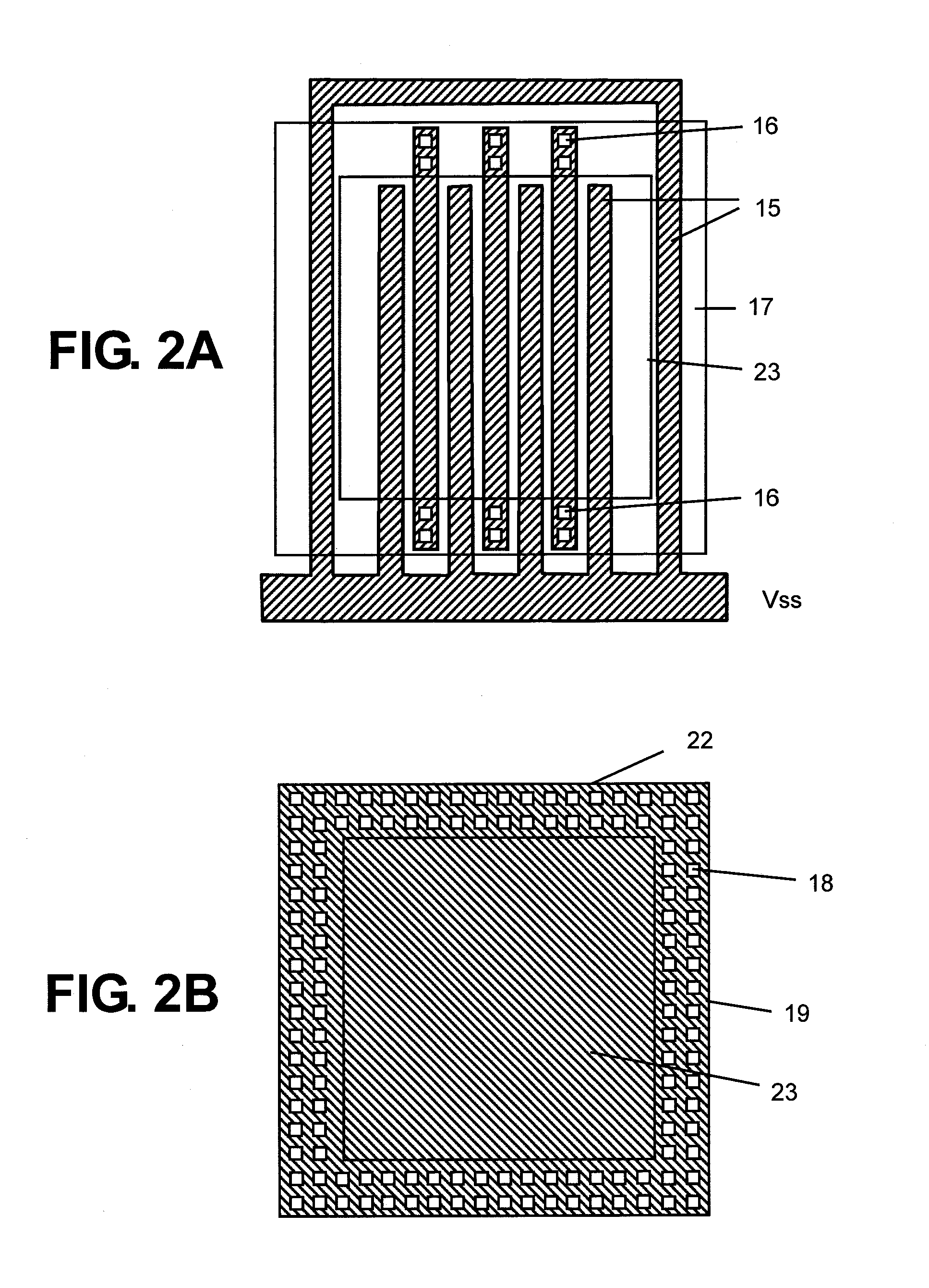
[0018]First, a pad structure of a semiconductor device according to the first embodiment of the present invention is described with reference to FIGS. 1A and 1B and FIGS. 2A and 2B. FIGS. 1A and 1B are plan views illustrating the pad structure of the semiconductor device. FIG. 1A illustrates a diffusion region, a gate electrode, a contact, and a pad opening, and FIG. 1B illustrates the diffusion region, a lower metal film, and the pad opening. FIGS. 2A and 2B are plan views illustrating the pad structure of the same semiconductor device as in FIGS. 1A and 1B. FIG. 2A illustrates the lower metal film, a first via, an intermediate metal film, and the pad opening, and FIG. 2B illustrates a second via, an upper metal film, and the pad opening.
[0019]As illustrated in FIG. 1A, a P-type diffusion region 10 for fixing a substrate potential and N-type diffusion regions 12 for a source and a drain are fo...
second embodiment
[0030]FIGS. 4A and 4B illustrate the present invention. FIG. 4A illustrates a diffusion region, a gate electrode, a contact, and a pad opening, and FIG. 4B illustrates the diffusion region, a lower metal film, and the pad opening. As illustrated in FIG. 4A, in the case where the NMOS transistor 21 has the source regions at both ends and at the center, in order to stabilize a substrate potential in the vicinity of the source and drain regions, the P-type diffusion region 10 for fixing the substrate potential can be formed along the center of the NMOS transistor 21 so as to be adjacent to the N-type diffusion region 12 for the source.
third embodiment
[0031]FIGS. 5A and 5B illustrate the present invention. FIG. 5A illustrates a diffusion region, a gate electrode, a contact, and a pad opening, and FIG. 5B illustrates the diffusion region, a lower metal film, and the pad opening. Although the NMOS transistor 21 of FIGS. 1A and 1B includes the N-type diffusion region 12 serving as the source as a diffusion region at the end in the gate length direction, the NMOS transistor 21 may include an N-type diffusion region 12 serving as the drain as illustrated in FIG. 5A.
[0032]The opening of the intermediate metal film 17 and the pad opening 23 only need to be rectangular, and may also be square or oblong.
[0033]Although the three-layered metal film including the lower metal film 15, the intermediate metal film 17, and the upper metal film 19 is used in the above description, a metal film of four or more layers may be used as appropriate. In this case, the metal film under the upper metal film needs to have a rectangular ring shape and inclu...
PUM
Abstract
Provided is a semiconductor device having high ESD tolerance. A first via (16) is used for electrically connecting a pad (22) to a drain of an NMOS transistor of an ESD protective circuit. The first vias (16) are formed under the pad (22) only on one side of a rectangular ring-shaped intermediate metal film (17) and on another side thereof opposed to the one side. In other words, all the first vias (16) for establishing an electrical connection to the drains are present substantially directly under the pad (22). Consequently, a surge current caused by ESD and applied to the pad (22) is more likely to flow uniformly among all the drains. Then, respective channels of the NMOS transistor of the ESD protective circuit are more likely to uniformly operate, and hence the ESD tolerance of the semiconductor device is increased.
Description
BACKGROUND OF THE INVENTION[0001]1. Field of the Invention[0002]The present invention relates to a semiconductor device including an NMOS transistor under a pad.[0003]2. Description of the Related Art[0004]A semiconductor device, also called an IC or a semiconductor chip, has a pad as an external connectionelectrode in order to establish an electrical connection to another element or another semiconductor device. In the vicinity of the pad, an ESD protective circuit is generally provided for protecting an internal circuit of the semiconductor device from electrostatic discharge (ESD). The ESD protective circuit uses a multi-finger NMOS transistor in many cases. In this case, a gate electrode, a source, and a back gate of the NMOS transistor are connected to a ground terminal, and a drain thereof is connected to the pad.[0005]By the way, various approaches are attempted for the ESD protective circuit using the multi-finger NMOS transistor so that respective channels may uniformly op...
Claims
Application Information
Patent Timeline
Application Date:The date an application was filed.
Publication Date:The date a patent or application was officially published.
First Publication Date:The earliest publication date of a patent with the same application number.
Issue Date:Publication date of the patent grant document.
PCT Entry Date:The Entry date of PCT National Phase.
Estimated Expiry Date:The statutory expiry date of a patent right according to the Patent Law, and it is the longest term of protection that the patent right can achieve without the termination of the patent right due to other reasons(Term extension factor has been taken into account ).
Invalid Date:Actual expiry date is based on effective date or publication date of legal transaction data of invalid patent.

