Power conversion apparatus

a power conversion apparatus and power technology, applied in the direction of motor/generator/converter stopper, dynamo-electric converter control, propulsion by batteries/cells, etc., can solve the problems of poor circuit reliability of large-capacity power transistors, insufficient surge suppression effect, uneven distance between silicon chips and snubber circuits, etc., to achieve improved long-term reliability, improve design efficiency, and suppress heat transfer

Inactive Publication Date: 2014-05-01
SUMITOMO HEAVY IND LTD
View PDF6 Cites 3 Cited by
  • Summary
  • Abstract
  • Description
  • Claims
  • Application Information

AI Technical Summary

Benefits of technology

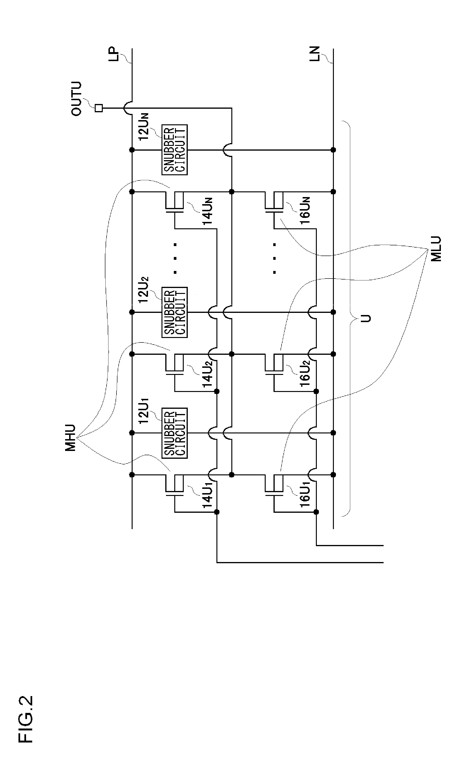
[0022]Such an embodiment suppresses heat transfer between adjacent layout units. That is to say, such an embodiment is capable of protecting the snubber circuit or the transistor included in each layout unit from heat generated by a transistor included in a different layout unit. Typically, repeated temperature changes lead to quick deterioration of a solder connection that connects circuit components or that connects a circuit component and a substrate. Such an embodiment relaxes the changes in the temperature, thereby providing improved long-term reliability.
[0023]Furthermore, the metal base substrate is divided into multiple sections in increments of layout units. Thus, in a case in which the designer designs several kinds of power conversion apparatuses configured to drive loads having different capacities, such an embodiment allows the designer to change the number of layout units in a simple manner. Thus, such an arrangement provides improved design efficiency without damaging the aforementioned advantages.

Problems solved by technology

Such a large-capacity power transistor can have a problem of poor circuit reliability when it is subjected to noise.
With such a configuration, the distance between each of the silicon chips and the snubber circuit is not uniform.
Thus, such an arrangement has a problem of an insufficient surge suppression effect with respect to transistors formed on a silicon chip which is arranged at a long electrical distance from the snubber circuit.
As the capacitance of a capacitor becomes greater, the frequency characteristics of the capacitor become poor.
This is why it is difficult for such an arrangement to suppress high-frequency surge noise.
Thus, with such an arrangement, there is a risk of vibration leading to deterioration in the long-term reliability of the circuit.

Method used


Image

  • Power conversion apparatus
  • Power conversion apparatus
  • Power conversion apparatus

Examples


first modification

[0060]FIG. 4 is a diagram showing a configuration of a power conversion apparatus 2a according to a first modification.

[0061]The metal base substrate 20 is configured as physically separate sections each provided for a corresponding one of the layout units 22U. The adjacent layout units 22U may be fixed by screws.

[0062]Such a modification is capable of suppressing heat transfer between adjacent layout units 22U. Specifically, such a modification is capable of protecting the transistor units 14U and 16U or otherwise the snubber circuit 12U included in each layout unit 22U from heat generated by a transistor included in a different layout unit 22U. Such an arrangement is capable of suppressing changes in the temperature of the transistor units, the snubber circuit, and solder connections included in the layout unit 22U. This suppresses deterioration of such components, thereby providing improved long-term reliability.

[0063]Furthermore, such a modification allows the number of layout u...

second modification

[0064]FIG. 5 is a diagram showing a configuration of a power conversion apparatus 2b according to a second modification.

[0065]In the metal base substrate 20, a pair of slits 24 is provided for each of the snubber circuits 12U1 through 12U4 such that each snubber circuit 12U is interposed between the slits arranged along the second direction Y.

[0066]With such a modification, directing attention to the snubber circuit 12Ui of a given layout unit 22Ui, one slit of the pair of slits 24 relaxes the thermal effects of the transistor units 14Ui and 16Ui of the same layout unit 22Ui. Furthermore, the other slit of the pair of slits 24 relaxes the thermal effects of the transistor units 14Uj and 16Uj of the adjacent layout unit 22Uj. Thus, such a modification provides improved long-term reliability.

[0067]The second modification may be combined with the first modification. That is to say, an arrangement may be made in which the metal base substrate 20 is divided in increments of layout units,...

third modification

[0068]FIG. 6 is a diagram showing a configuration of a power conversion apparatus 2c according to a third modification.

[0069]With such a modification, the high-side transistor unit 14U and the low-side transistor unit 16U each include two sub-transistor units 26 and 28 adjacent to each other along the first direction X.

[0070]The metal base substrate 20 is divided in increments of high-side transistor units 14U and low-side transistor units 16U, instead of being divided in increments of layout units 22U.

[0071]Such a modification also provides the same advantages as those provided by the embodiment. Furthermore, by dividing the metal base substrate 20 into multiple sections, such a modification provides the same advantages as those provided by the first modification.

[0072]It should be noted that the terms “sub-transistor unit” and “transistor unit” are assigned for convenience of description. The sub-transistor units shown in FIG. 6 correspond in function to the transistor units shown...


PUM


Abstract

A high-side transistor includes N (N represents an integer of two or more) high-side transistor units electrically arranged in parallel between a high-side power supply line and an output terminal for the corresponding phase. A low-side transistor includes N low-side transistor units electrically arranged in parallel between a low-side power supply line and an output terminal for the corresponding phase. A snubber circuit is provided for each pair of a high-side transistor unit and a corresponding low-side transistor unit. The high-side transistor, the low-side transistor, and the N snubber circuits are mounted on a metal base substrate.

Description

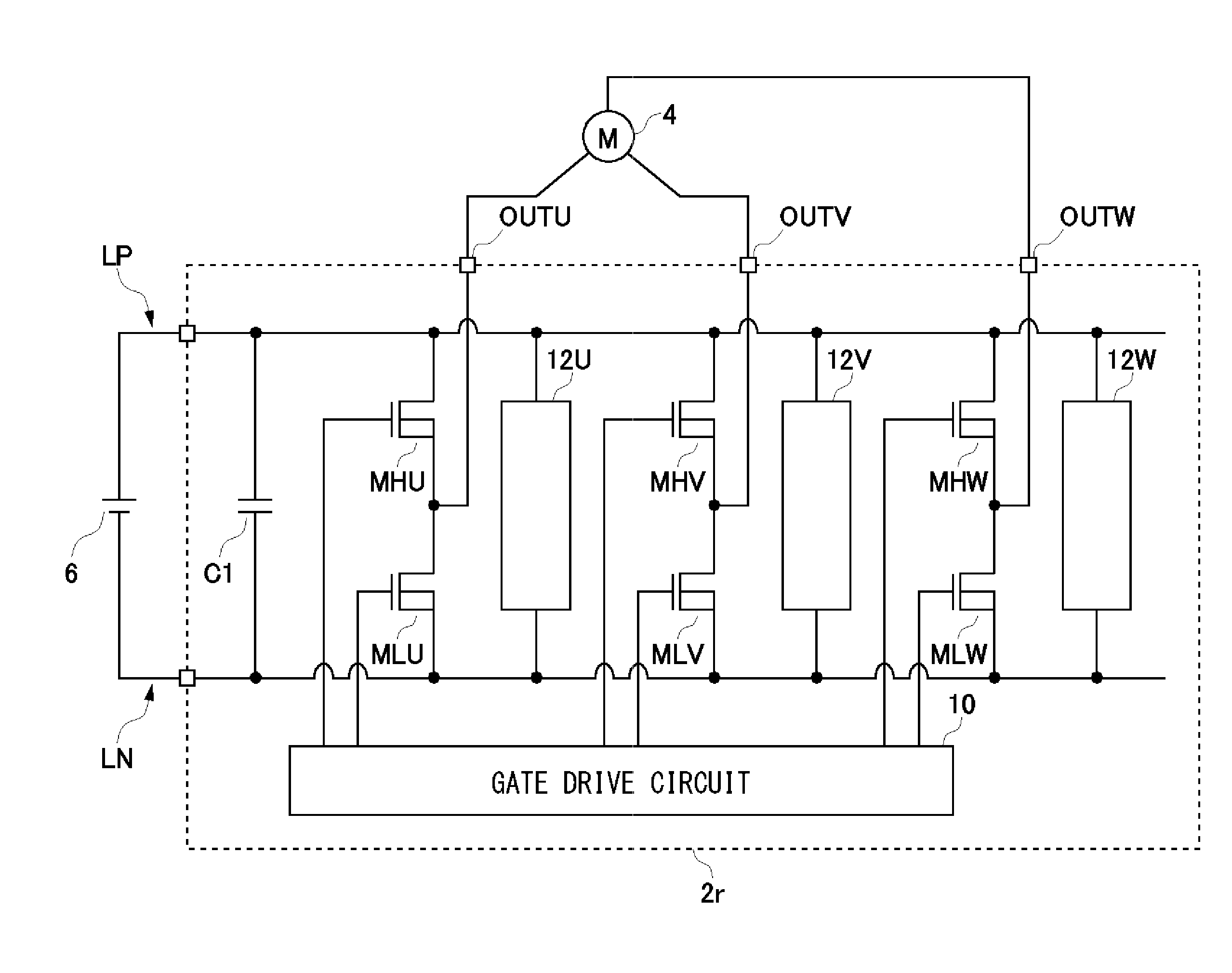
BACKGROUND OF THE INVENTION[0001]1. Field of the Invention[0002]The present invention relates to a power conversion apparatus.[0003]2. Description of the Related Art[0004]FIG. 1 is a circuit diagram showing a typical configuration of an electric power conversion apparatus (inverter) 2. The electric power conversion apparatus 2 is used to drive a load 4 such as an electric motor. The electric power conversion apparatus 2 includes: high-side transistors MHU, MHV, and MHW, respectively provided for the U phase, V phase, and W phase; low-side transistors MLU, MLV, and MLW, respectively provided for the U phase, V phase, and W phase; a gate drive circuit 10 which drives the high-side transistors MHU, MHV, and MHW and the low-side transistors MLU, MLV, and MLW for the respective phases; and snubber circuits 12U, 12V and 12W for the respective phases.[0005]In a case in which a large current is supplied to a load, the high-side transistor MH and the low-side transistor ML are each configure...

Claims


Application Information

Patent Timeline
Patent Type & Authority Applications(United States)
IPC IPC(8): B60L11/18
CPCB60L11/1803H02M7/003B60L2200/42Y02P90/60B60L50/51Y02T10/70
Inventor TASAKA, YASUHISAKIMIJIMA, KENICHI
Owner SUMITOMO HEAVY IND LTD
Why Eureka
Try Eureka