Metal-Gate MOS Transistor and Method of Forming the Transistor with Reduced Gate-to-Source and Gate-to-Drain Overlap Capacitance

a metal-gate mos transistor and overlap capacitance technology, which is applied in the field of metal-gate mos transistors, can solve the problems of increasing achieve the effects of reducing the gate-to-source and gate-to-drain overlap capacitance, reducing the width, and reducing the width

Active Publication Date: 2014-05-08
TEXAS INSTR INC
View PDF1 Cites 5 Cited by
  • Summary
  • Abstract
  • Description
  • Claims
  • Application Information

AI Technical Summary

Benefits of technology

[0050]One of the advantages of the present invention is that metal gate 230 / 380 is separated from the source and drain regions 220 / 350 and 222 / 352 by a larger distance than the distance that separates metal gate 130 from the source and drain regions 120 and 122. The larger the separation distance, in turn, the more the overlap capacitance is reduced.

Problems solved by technology

One of the problems with MOS transistor 100 is that high-k gate dielectric structure 126 substantially increases the gate-to-source and gate-to-drain overlap capacitance.

Method used


Image

  • Metal-Gate MOS Transistor and Method of Forming the Transistor with Reduced Gate-to-Source and Gate-to-Drain Overlap Capacitance
  • Metal-Gate MOS Transistor and Method of Forming the Transistor with Reduced Gate-to-Source and Gate-to-Drain Overlap Capacitance
  • Metal-Gate MOS Transistor and Method of Forming the Transistor with Reduced Gate-to-Source and Gate-to-Drain Overlap Capacitance

Examples


Embodiment Construction

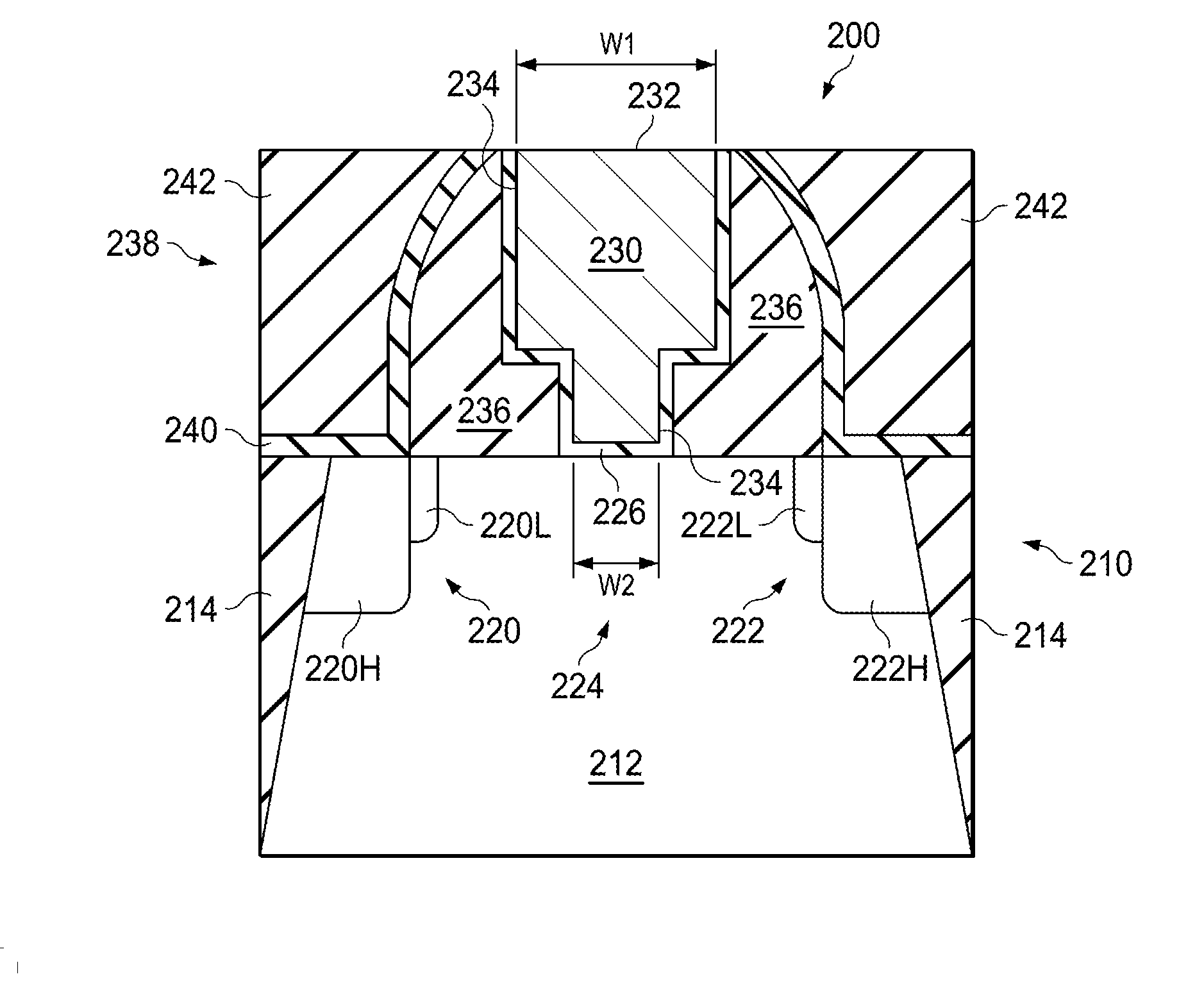
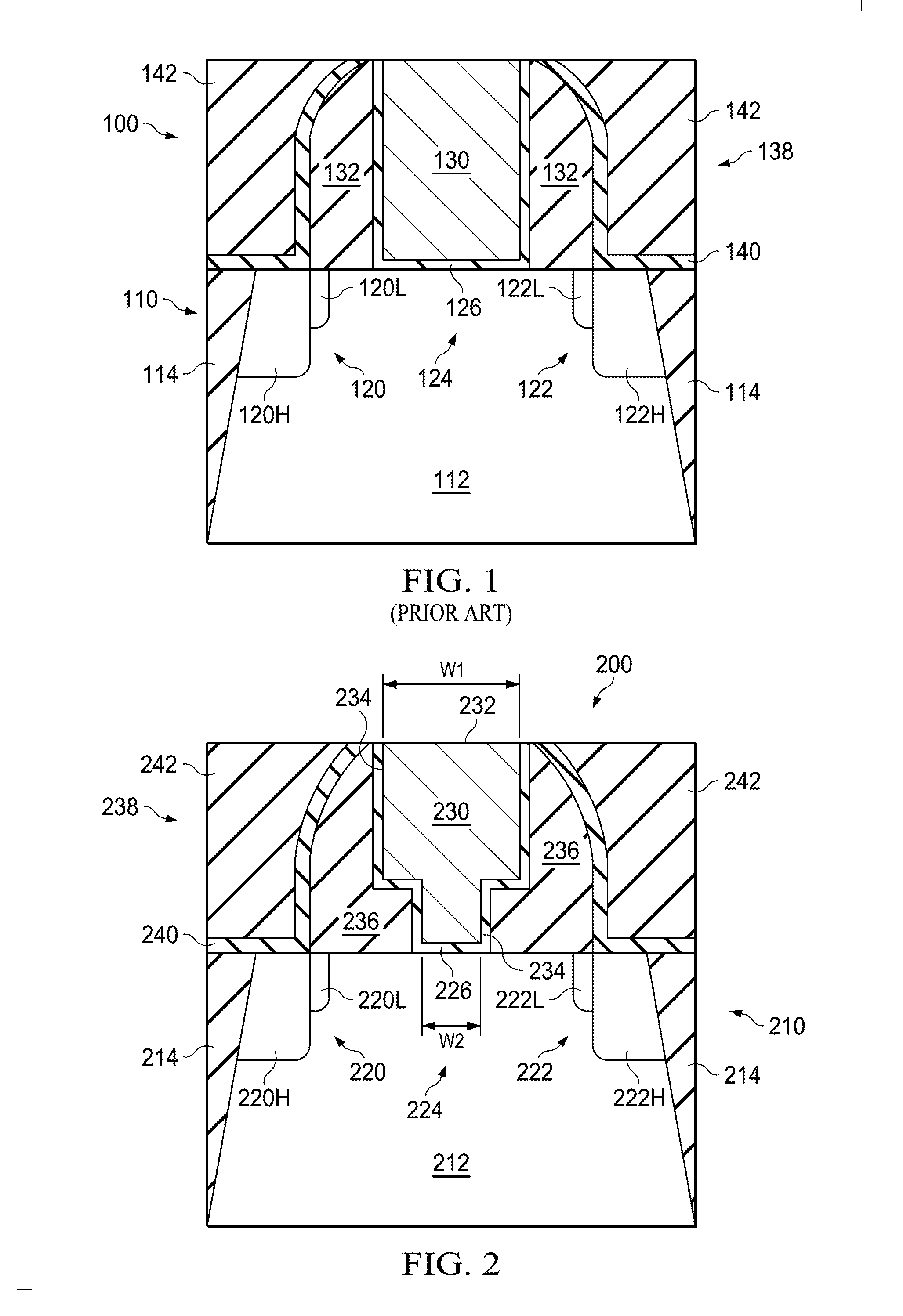
[0020]FIG. 2 shows a cross-sectional view that illustrates an example of a metal-gate MOS transistor 200 in accordance with the present invention. As described in greater detail below, the present invention reduces the gate-to-source and gate-to-drain overlap capacitance by forming the high-k gate dielectric along the inside of a sidewall structure which has been formed to lie further away from the source and the drain.

[0021]As shown in FIG. 2, MOS transistor 200 includes a semiconductor body 210. Semiconductor body 210, in turn, includes a single-crystal-silicon substrate region 212, and a trench isolation structure 214 that touches substrate region 212. In addition, semiconductor body 210 includes a source 220 and a drain 222 that each touch substrate region 212.

[0022]The source 220 and drain 222, which are spaced apart, each has a conductivity type that is the opposite of the conductivity type of substrate region 212. Source 220 includes a lightly-doped region 220L, and a heavily...


PUM


Abstract

The gate-to-source and gate-to-drain overlap capacitance of a MOS transistor with a metal gate and a high-k gate dielectric are reduced by forming the high-k gate dielectric along the inside of a sidewall structure which has been formed to lie further away from the source and the drain.

Description

BACKGROUND OF THE INVENTION[0001]1. Field of the Invention[0002]The present invention relates to metal-gate MOS transistors and, more particularly, to a metal-gate MOS transistor and a method of forming the transistor with reduced gate-to-source and gate-to-drain overlap capacitance.[0003]2. Description of the Related Art[0004]A metal oxide semiconductor (MOS) transistor is a well-known semiconductor device which can be implemented as either an n-channel (NMOS) device or a p-channel (PMOS) device. A MOS transistor has spaced-apart source and drain regions, which are separated by a channel, and a gate that lies over, and is insulated from, the channel by a gate dielectric layer. A metal-gate MOS transistor is a type of MOS transistor that utilizes a metal gate and a high-k gate dielectric layer.[0005]FIG. 1 shows a cross-sectional view that illustrates a prior-art metal-gate MOS transistor 100. As shown in FIG. 1, MOS transistor 100 includes a semiconductor body 110. Semiconductor bo...

Claims


Application Information

Patent Timeline
Patent Type & Authority Applications(United States)
IPC IPC(8): H01L29/78H01L21/336
CPCH01L21/28114H01L29/42376H01L29/4966H01L29/517H01L29/66545H01L29/6656H01L29/6659H01L29/7833H01L29/0653H01L29/495H01L29/78
Inventor MEHROTRA, MANOJNIIMI, HIROAKI
Owner TEXAS INSTR INC
Why Eureka
Try Eureka