Process for manufacturing a lid for an electronic device package, and lid for an electronic device package

a technology for electronic devices and manufacturing processes, applied in the direction of microstructural devices, coatings, microstructure systems, etc., can solve the problems of affecting the performance the failure of the protective lid, and the failure of the electronic device packag

Active Publication Date: 2014-05-15
STMICROELECTRONICS INT NV
View PDF14 Cites 7 Cited by
  • Summary
  • Abstract
  • Description
  • Claims
  • Application Information

AI Technical Summary

Benefits of technology

[0011]One or more embodiments of the present invention is to provide a process for manufacturing a lid for an electronic device package, a process for manufacturing a packaged microelectromechanical device, a lid for an electronic device package, and a packaged microelectromechanical device that allow to overcome the limitations described and, in particular, enable use of soldering pastes eliminating or at least reducing the risk of migration of molten soldering paste in cavities for housing the microelectromechanical devices during final assembly.

Problems solved by technology

Given that the extremely marked miniaturization of MEMS devices entails a certain fragility of micromechanical structures, it is common to use protective lids that encapsulate the parts more readily subject to failure.
In particular, in many cases, the transmission of the signals may be disturbed by the environment, and hence it is necessary to envisage a protection from light and electromagnetic interference.
However, soldering pastes melt during the steps of assembly of a package (comprising supporting board, MEMS sensor, and lid) to the boards of the electronic system in which the MEMS sensor is to be used.
Molten soldering pastes tend to climb up the vertical conductive walls of the lid, invading the cavities in which the MEMS sensor is housed and leaving empty spaces in the soldering joints.
The empty spaces in the soldering joints are particularly undesirable, because, on the one hand, they weaken soldering and, on the other, may cause leakages that affect the performance of the devices, especially when a controlled-pressure reference chamber is desired.

Method used


Image

  • Process for manufacturing a lid for an electronic device package, and lid for an electronic device package
  • Process for manufacturing a lid for an electronic device package, and lid for an electronic device package
  • Process for manufacturing a lid for an electronic device package, and lid for an electronic device package

Examples


Embodiment Construction

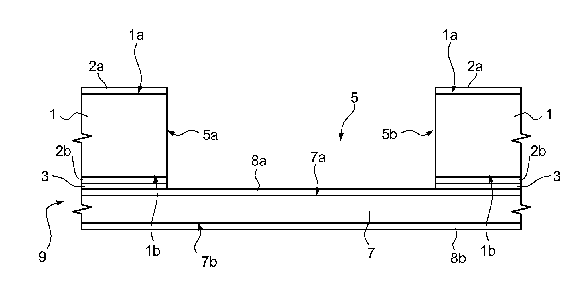
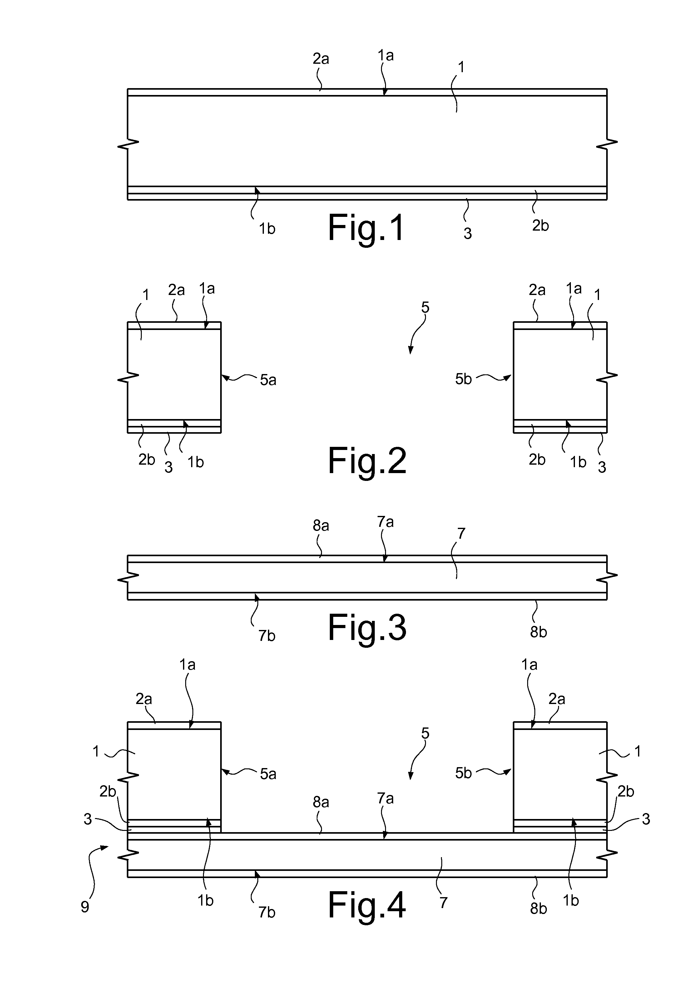
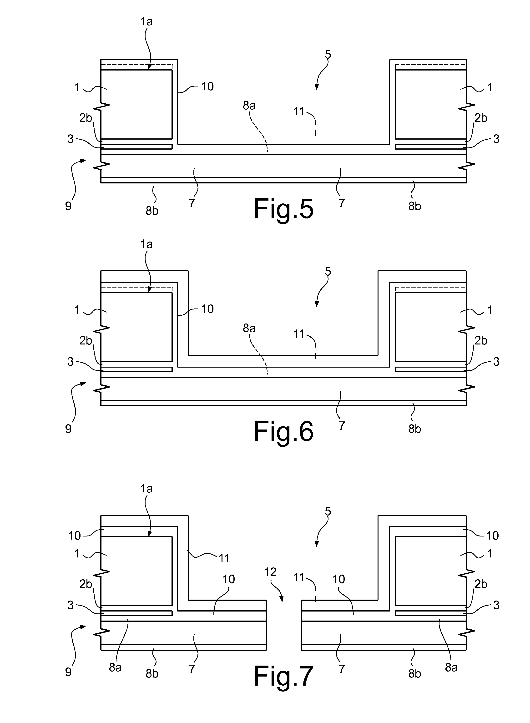
[0030]In an initial step of a process for manufacturing a packaged microelectromechanical device, to which FIG. 1 refers, a first face 1a and a second face 1b of a first protective substrate 1 are coated, respectively, with a first conductive layer 2a and a second conductive layer 2b, both made of metal, in particular copper. In one embodiment, the first protective substrate is made of an organic material, for example bismaleimide triazine (BT). Moreover, an adhesive layer 3 is laminated on the second conductive layer 2b.

[0031]Next (FIG. 2), a through cavity 5 is formed in the first conductive layer 2a, in the first protective substrate 1, in the second conductive layer 2b, and in the adhesive layer 3, for example by through punching.

[0032]As illustrated in FIG. 3, a second protective substrate 7, which has a smaller thickness than the first protective substrate 1 and is made of the same material, is prepared separately. In particular, a first face 7a and a second face 7b of the se...


PUM

PropertyMeasurementUnit
metallicaaaaaaaaaa
fragilityaaaaaaaaaa
mechanicalaaaaaaaaaa

Abstract

A process for manufacturing a packaged microelectromechanical device includes: forming a lid having a face and a cavity open on the face; coating the face of the lid and walls of the cavity with a metal layer containing copper; and coating the metal layer with a protective layer.

Description

BACKGROUND[0001]1. Technical Field[0002]The present invention relates to a process for manufacturing a lid for an electronic device package, to a process for manufacturing a packaged microelectromechanical device, to a lid for an electronic device package, and to a packaged microelectromechanical device.[0003]2. Description of the Related Art[0004]MEMS (microelectromechanical systems) devices find increasingly extensive use in a wide range of sectors as miniaturized sensors or transducers. For example, microphones and pressure sensors are frequently used in mobile communication devices and filming apparatuses, such as cell phones and video cameras.[0005]Given that the extremely marked miniaturization of MEMS devices entails a certain fragility of micromechanical structures, it is common to use protective lids that encapsulate the parts more readily subject to failure. Normally, MEMS sensors or transducers are mounted on substrates, possibly with control circuits. The substrates are ...

Claims


Application Information

Patent Timeline
Patent Type & Authority Applications(United States)
IPC IPC(8): B81C1/00B81B3/00
CPCB81B3/0018B81C1/00261B81C2203/035B81C1/00269B81B2201/0257B81B2207/093B81C2203/0109H01L2224/48137H01L2224/48227H01L2924/15151H01L2224/48091H01L2924/00014
Inventor GRITTI, ALEXCREMA, PAOLO
Owner STMICROELECTRONICS INT NV
Why Eureka
Try Eureka