
Method for Forming Insulation Film Using Non-Halide Precursor Having Four or More Silicons

a technology of non-halide precursors and insulation films, which is applied in the direction of coatings, metallic material coating processes, chemical vapor deposition coatings, etc., can solve the problems of unwanted deposition inside the exhaust pipe or particles, the use of halide precursors is associated, and the above methods face not only the cost increase problem but also the productivity decrease problem, so as to improve chemical adsorption

Active Publication Date: 2014-05-22
ASM IP HLDG BV
View PDF5 Cites 397 Cited by
  • Summary
  • Abstract
  • Description
  • Claims
  • Application Information

AI Technical Summary

Benefits of technology

The present invention proposes the use of non-halide precursors to overcome the problems caused by using halide precursors in depositing films like SiN, SiCN, and a-Si by PEALD. The study found that non-halide precursors have better chemical adsorption and can form high-quality films with good step coverage. The use of non-halide precursors also solves the problem of temperature-dependent unwanted accumulations of by-products and reactivity with reactant gas.

Problems solved by technology

Since the reactivity of NH3 or H2 with a halide precursor is very high, unwanted deposition occurs inside an exhaust pipe or particles are generated as a result of mixing with other gases when a process takes place.
Accordingly, the above methods face not only the cost increase problem but also the productivity decrease problem due to the process sequence being more complex and the process duration being prolonged.
However, the use of halide precursors is associated with the problems discussed above.
When evaluating non-halide precursors for depositing films constituted by SiN, SiCN, and a-Si, it was observed that chemical adsorption thereof was often blocked during a process of depositing the films.

Method used


Image

  • Method for Forming Insulation Film Using Non-Halide Precursor Having Four or More Silicons
  • Method for Forming Insulation Film Using Non-Halide Precursor Having Four or More Silicons
  • Method for Forming Insulation Film Using Non-Halide Precursor Having Four or More Silicons

Examples


example

Method and Conditions

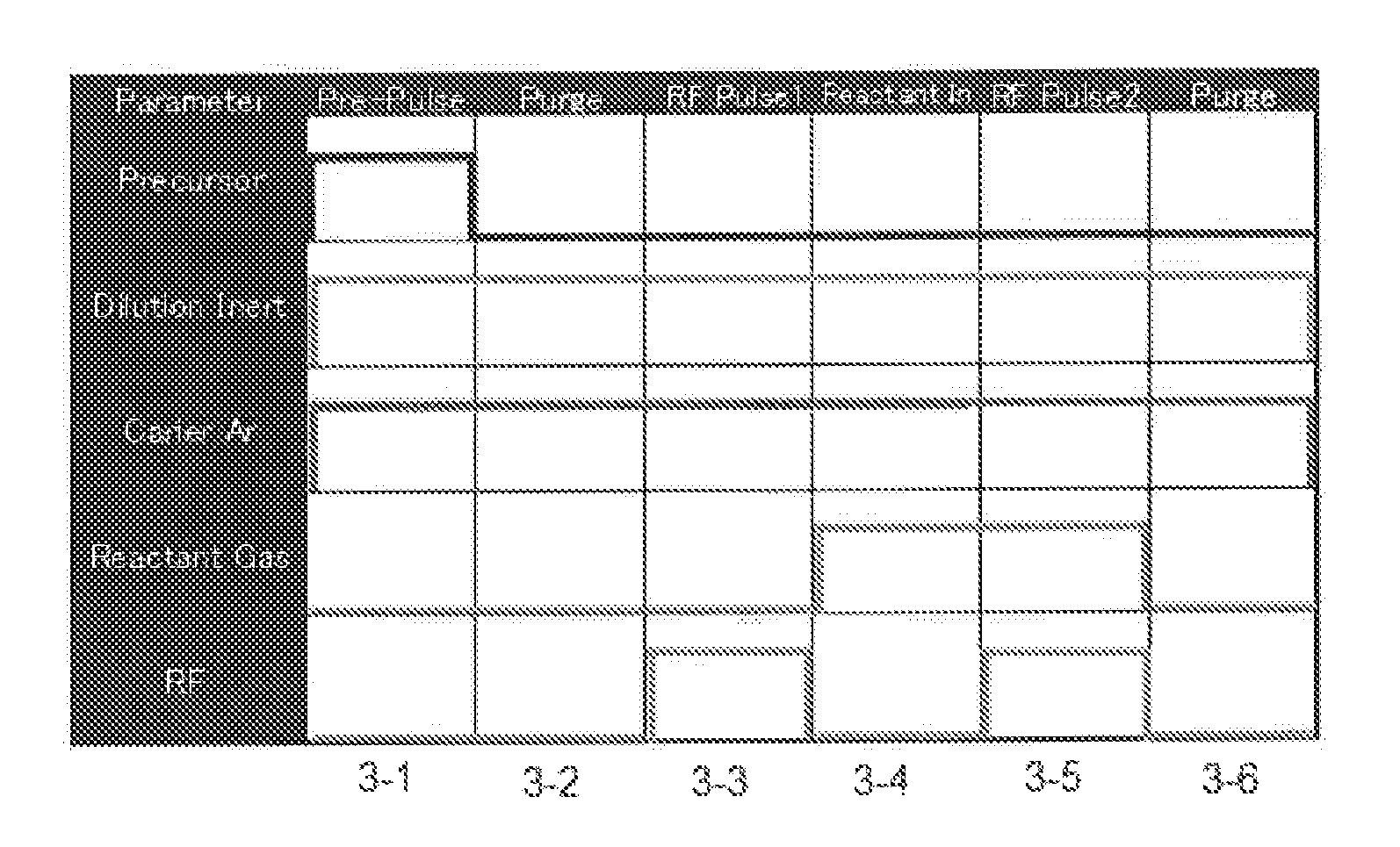
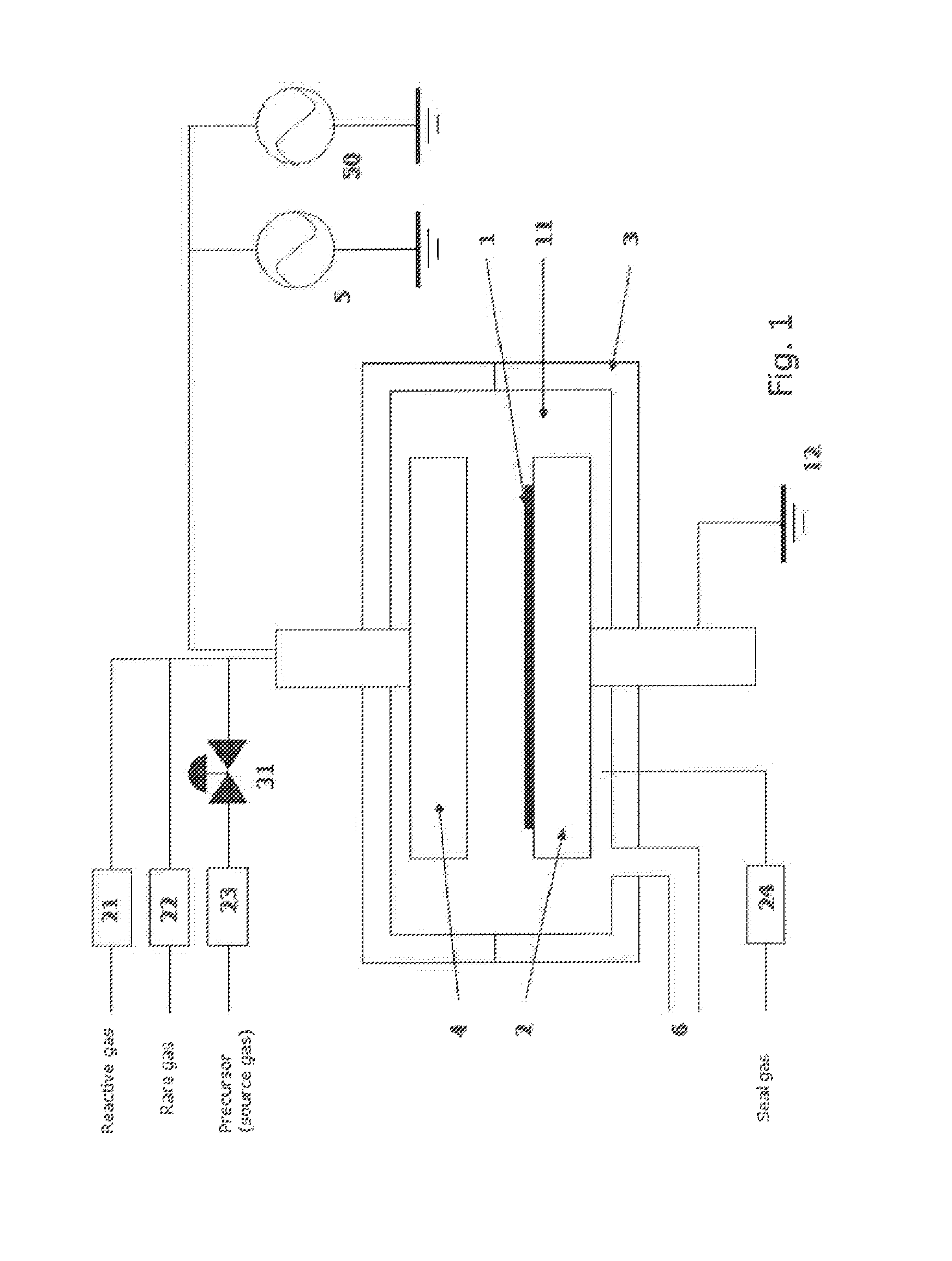
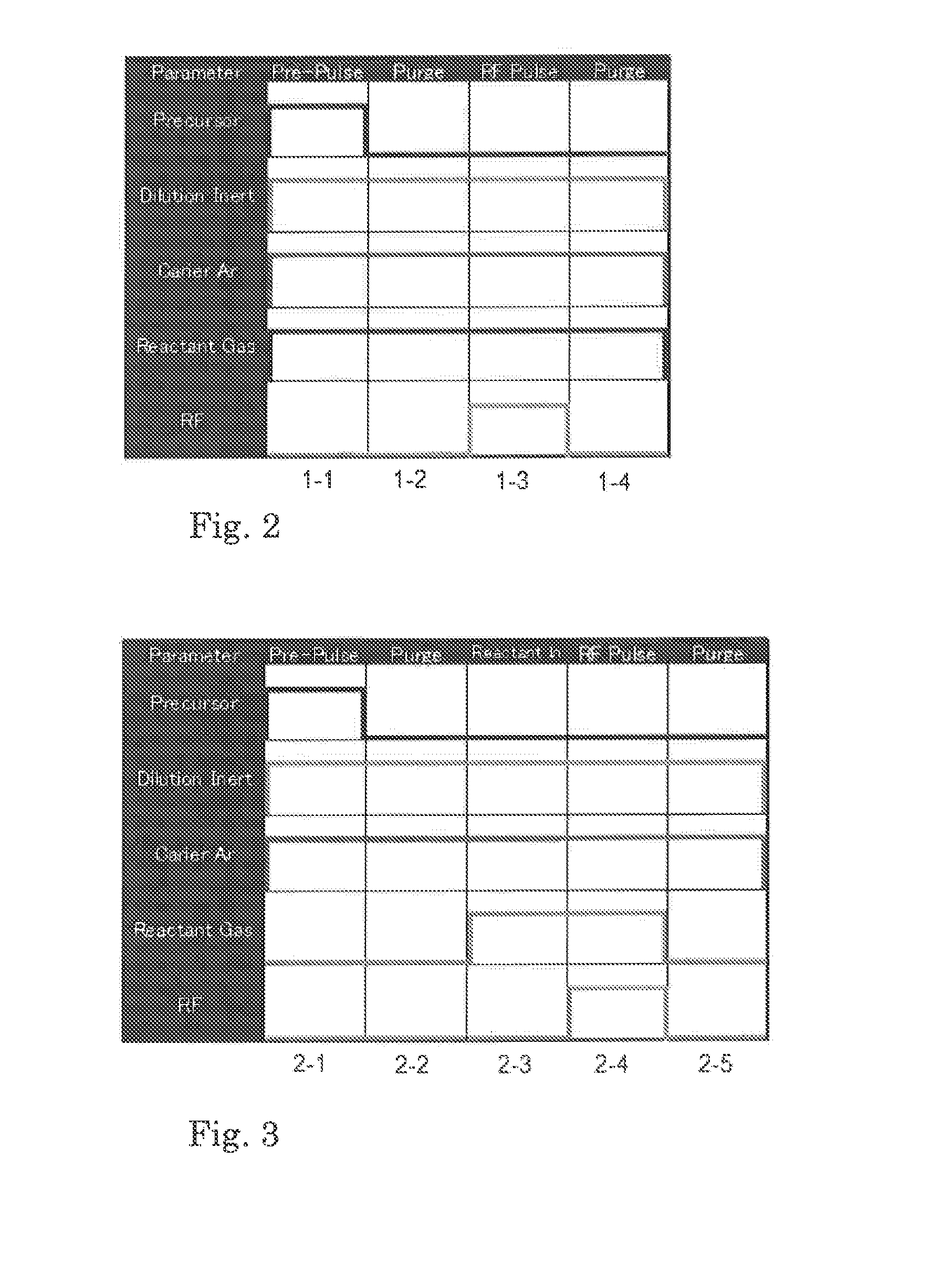
[0057]Insulation films (SiN, SiCN, and a-Si) were each formed on a 300-mm substrate having a patterned surface having an aspect ratio of about 2 and an opening width of about 50 nm under the conditions shown below using Sequences 1 to 3 illustrated in FIGS. 2, 3, and 4, respectively, and the apparatus illustrated in FIG. 1. The thickness of film was 30 nm for evaluating film properties. The conditions of PEALD are shown in Tables 2 and 3 below:

TABLE 2Sequence 1Sequence 2Sequence 3StepDuration (sec.)StepDuration (sec.)StepDuration (sec.)1-10.52-10.53-10.51-212-213-211-312-323-311-40.32-413-422-50.33-513-60.3

TABLE 3Reactant:DilutionRFPGTEXPrecursorSQFilm(SLM)(SLM)(W)(Pa)(min)(° C.)0Hexachlorodisilane1 SiNNH3: 3Ar: 1200300124000′Hexachlorodisilane1 SiNNH3: 3Ar: 1200300121000″Hexachlorodisilane1 SiNH2 / N2: 1Ar: 1200300121001Cyclopentasilane1 SiNNH3: 3Ar: 1400300124002Cyclopentasilane2 SiNNH3: 3Ar: 1400300124003Cyclopentasilane1 SiNN2 / H2: 3Ar: 1400300121004Cyclopentas...


PUM

PropertyMeasurementUnit
temperatureaaaaaaaaaa
thicknessaaaaaaaaaa
thicknessaaaaaaaaaa

Abstract

A method of forming an insulation film on a semiconductor substrate by plasma enhanced atomic layer deposition (PEALD), includes: (i) adsorbing a non-excited non-halide precursor having four or more silicon atoms in its molecule onto a substrate placed in a reaction space; (ii) supplying an oxygen-free reactant to the reaction space without applying RF power so as to expose the precursor-adsorbed substrate to the reactant; and (iii) after step (ii), applying RF power to the reaction space while the oxygen-free reactant is supplied in the reaction space; and (iv) repeating steps (i) to (iii) as a cycle, thereby depositing an insulation film on the substrate.

Description

BACKGROUND[0001]1. Field of the Invention[0002]The present invention relates generally to semiconductor integrated circuit manufacturing and, more particularly, to a method for forming a conformal insulation film constituted by, e.g., amorphous silicon or silicon nitride on a semiconductor substrate by plasma-enhanced atomic layer deposition (PEALD).[0003]2. Description of the Related Art[0004]For forming a silicon nitride by atomic layer deposition (ALD), a halide precursor is often used. This is because a halide precursor, especially a precursor containing chlorine, is characterized by its easy substitution treatment by heat reaction with NH3. Since the reactivity of NH3 or H2 with a halide precursor is very high, unwanted deposition occurs inside an exhaust pipe or particles are generated as a result of mixing with other gases when a process takes place. Thus, to deal with the above problems, extra attention needs to be paid to the process conditions, and special modifications to...

Claims


Application Information

Patent Timeline
Patent Type & Authority Applications(United States)
IPC IPC(8): H01L21/02
CPCH01L21/02211H01L21/02274H01L21/0228C23C16/24C23C16/345C23C16/36C23C16/45542H01L21/32055H01L21/02167H01L21/0217
Inventor FUKAZAWA, ATSUKIFUKUDA, HIDEAKI
Owner ASM IP HLDG BV
Learn More