Method for forming insulation film using non-halide precursor having four or more silicons

a technology of non-halide precursors and insulation films, applied in the direction of chemical vapor deposition coatings, coatings, plasma techniques, etc., can solve the problems of unwanted deposition inside the exhaust pipe or particles, the use of halide precursors is associated, and the above methods face not only the cost increase problem, but also the productivity decrease problem. achieve the effect of improving chemical adsorption

a technology of non-halide precursors and insulation films, applied in the direction of chemical vapor deposition coatings, coatings, plasma techniques, etc., can solve the problems of unwanted deposition inside the exhaust pipe or particles, the use of halide precursors is associated, and the above methods face not only the cost increase problem, but also the productivity decrease problem. achieve the effect of improving chemical adsorption

US8784951B2Active Publication Date: 2014-07-22ASM IP HLDG BV

Image

  • Method for forming insulation film using non-halide precursor having four or more silicons
  • Method for forming insulation film using non-halide precursor having four or more silicons
  • Method for forming insulation film using non-halide precursor having four or more silicons

Examples


example

Method and Conditions

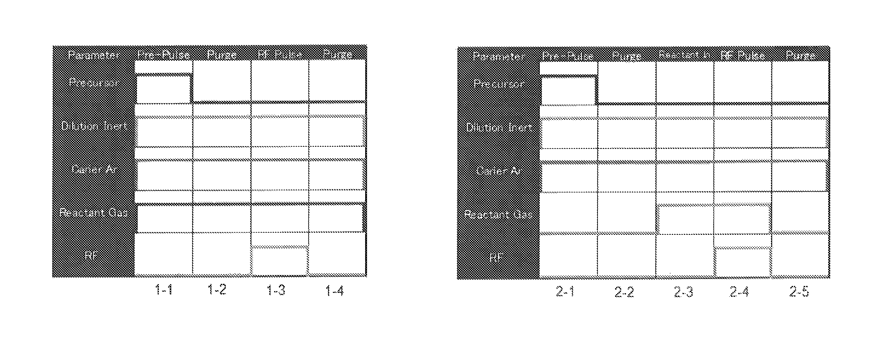
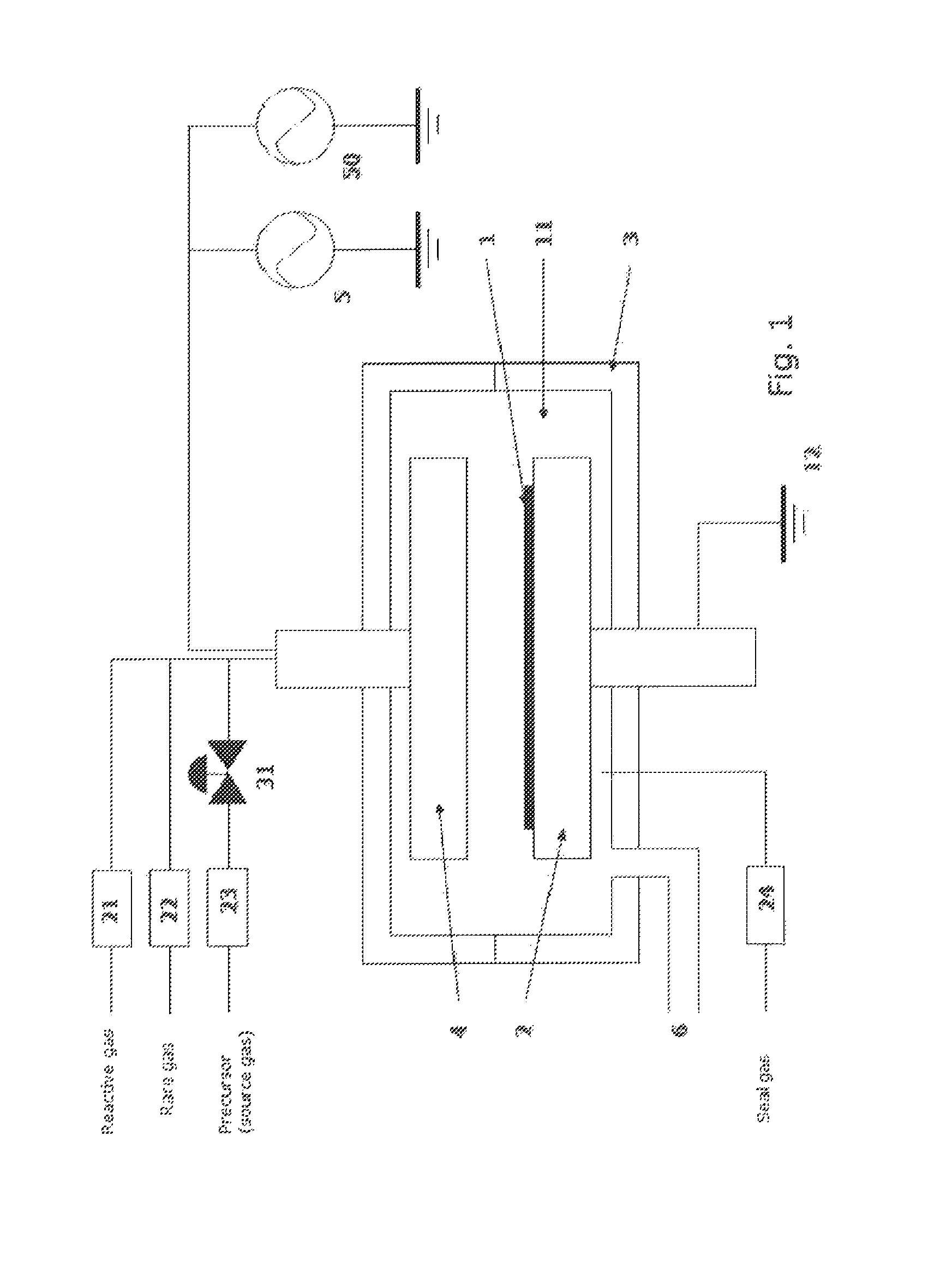
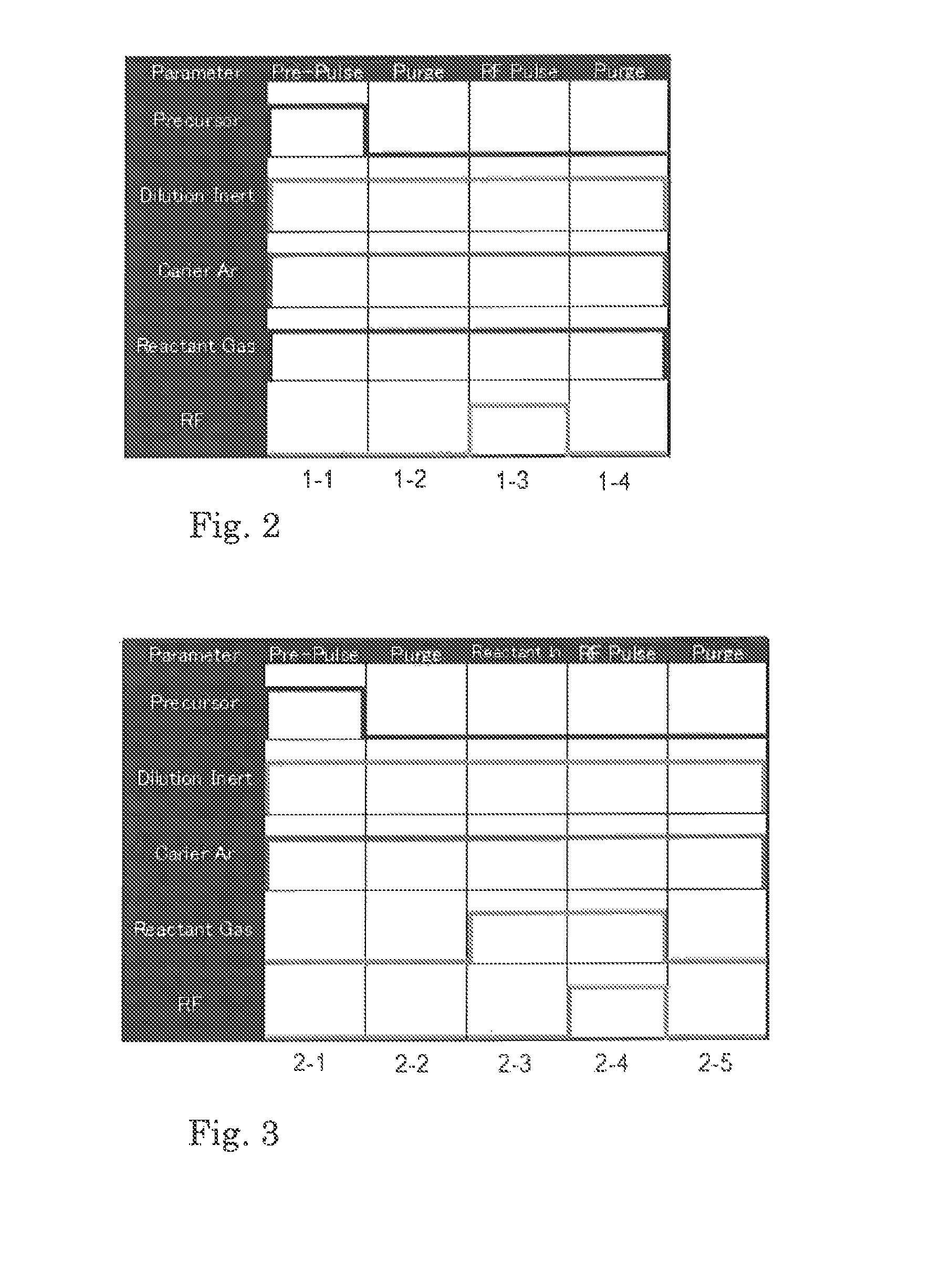
[0058]Insulation films (SiN, SiCN, and a-Si) were each formed on a 300-mm substrate having a patterned surface having an aspect ratio of about 2 and an opening width of about 50 nm under the conditions shown below using Sequences 1 to 3 illustrated in FIGS. 2, 3, and 4, respectively, and the apparatus illustrated in FIG. 1. The thickness of film was 30 nm for evaluating film properties. The conditions of PEALD are shown in Tables 2 and 3 below:

[0059]

TABLE 2Sequence 1Sequence 2Sequence 3StepDuration (sec.)StepDuration (sec.)StepDuration (sec.)1-10.52-10.53-10.51-212-213-211-312-323-311-40.32-413-422-50.33-513-60.3

[0060]

TABLE 3Reactant:DilutionRFPGTEXPrecursorSQFilm(SLM)(SLM)(W)(Pa)(min)(° C.)0Hexachlorodisilane1 SiNNH3: 3Ar: 1200300124000′Hexachlorodisilane1 SiNNH3: 3Ar: 1200300121000″Hexachlorodisilane1 SiNH2 / N2: 1Ar: 1200300121001Cyclopentasilane1 SiNNH3: 3Ar: 1400300124002Cyclopentasilane2 SiNNH3: 3Ar: 1400300124003Cyclopentasilane1 SiNN2 / H2: 3Ar: 140030012100...


PUM

PropertyMeasurementUnit
temperatureaaaaaaaaaa
thicknessaaaaaaaaaa
thicknessaaaaaaaaaa

Abstract

A method of forming an insulation film on a semiconductor substrate by plasma enhanced atomic layer deposition (PEALD), includes: (i) adsorbing a non-excited non-halide precursor having four or more silicon atoms in its molecule onto a substrate placed in a reaction space; (ii) supplying an oxygen-free reactant to the reaction space without applying RF power so as to expose the precursor-adsorbed substrate to the reactant; and (iii) after step (ii), applying RF power to the reaction space while the oxygen-free reactant is supplied in the reaction space; and (iv) repeating steps (i) to (iii) as a cycle, thereby depositing an insulation film on the substrate.

Description

BACKGROUND[0001]1. Field of the Invention[0002]The present invention relates generally to semiconductor integrated circuit manufacturing and, more particularly, to a method for forming a conformal insulation film constituted by, e.g., amorphous silicon or silicon nitride on a semiconductor substrate by plasma-enhanced atomic layer deposition (PEALD).[0003]2. Description of the Related Art[0004]For forming a silicon nitride by atomic layer deposition (ALD), a halide precursor is often used. This is because a halide precursor, especially a precursor containing chlorine, is characterized by its easy substitution treatment by heat reaction with NH3. Since the reactivity of NH3 or H2 with a halide precursor is very high, unwanted deposition occurs inside an exhaust pipe or particles are generated as a result of mixing with other gases when a process takes place. Thus, to deal with the above problems, extra attention needs to be paid to the process conditions, and special modifications to...

Claims


Application Information

Patent Timeline
22 Jul 2014
Publication
US8784951B2
IPC
C23C16/505; C23C16/50; C23C16/36; C23C16/34; H01L21/31; H01L21/02; C23C16/24; C23C16/32; C23C16/00
CPC
H01L21/0217; C23C16/24; H01L21/0228; H01L21/02274; H01L21/02211; C23C16/36; H01L21/02167; C23C16/45542
Inventors
FUKAZAWA, ATSUKI; FUKUKA, HIDEAKI