Semiconductor device
a semiconductor device and semiconductor technology, applied in semiconductor devices, instruments, computing, etc., can solve the problems of reducing the field-effect mobility of a transistor or an increase in off-state current, degrading the electrical characteristics of a transistor, and affecting the operation of the device, so as to achieve stable electrical characteristics, small variation in electrical characteristics, and high reliability
- Summary
- Abstract
- Description
- Claims
- Application Information
AI Technical Summary
Benefits of technology
Problems solved by technology
Method used
Image

Examples
embodiment 1
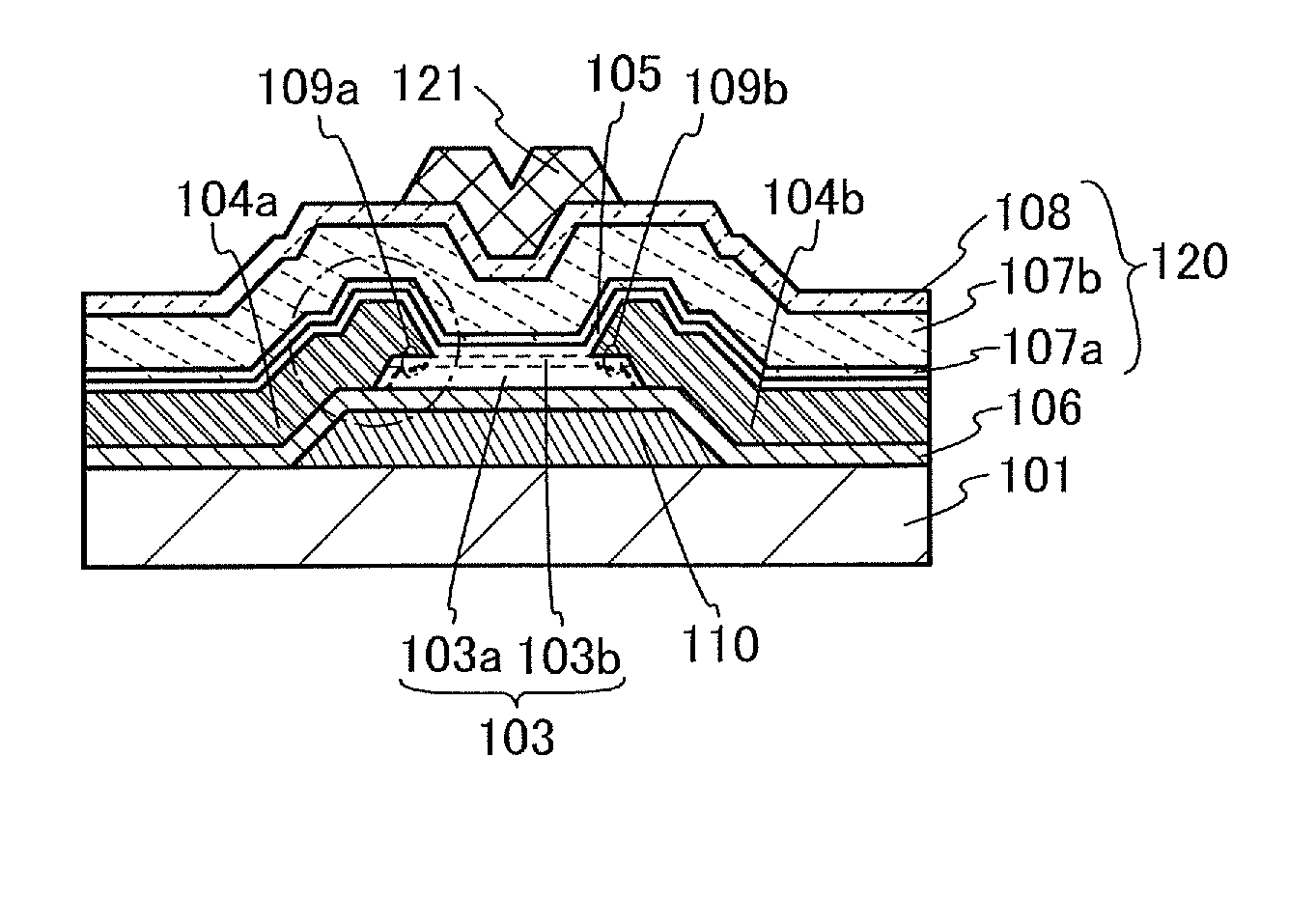
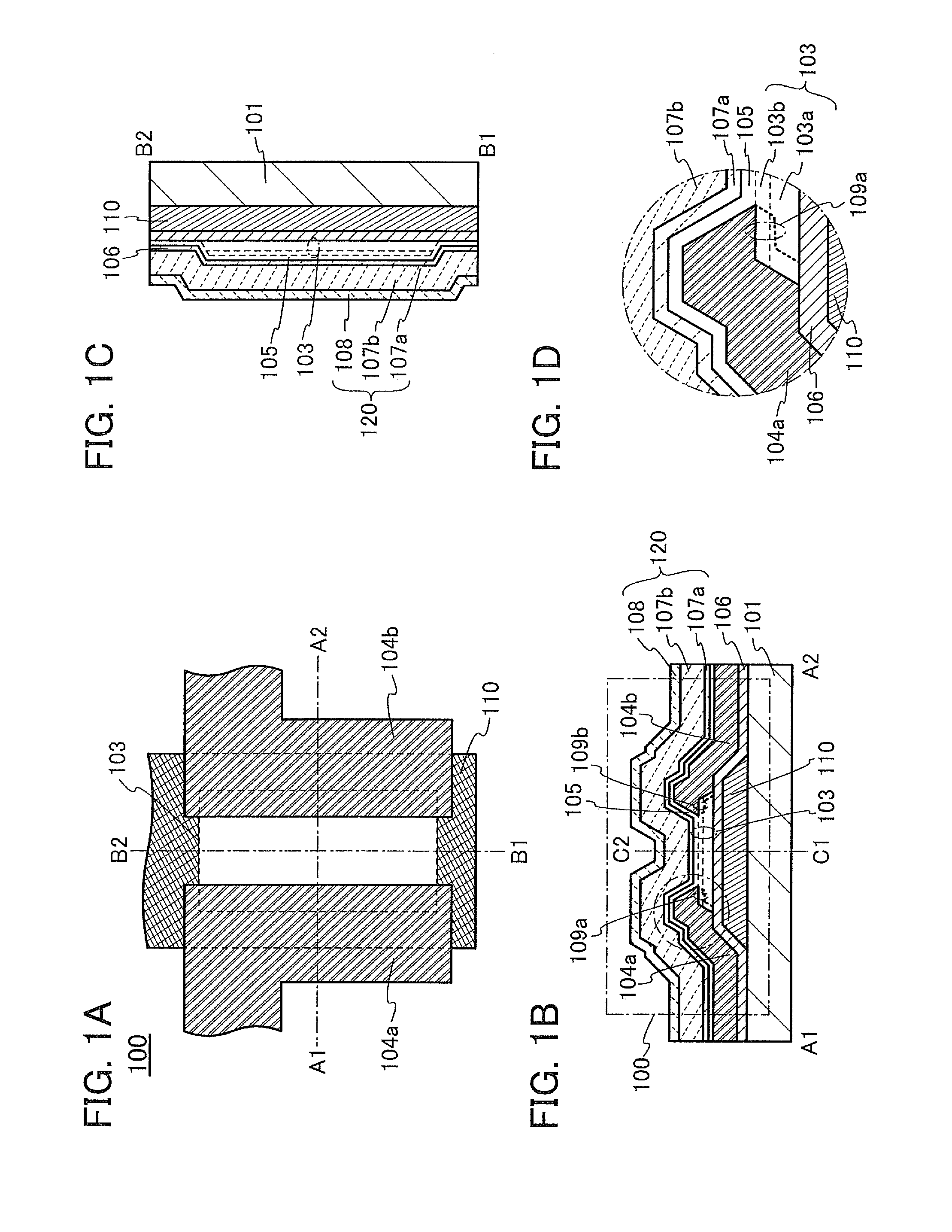
[0070]In this embodiment, as an example of one embodiment of a semiconductor device, a transistor 100 is described.
[0071]FIGS. 1A to 1D show the transistor 100 which is one embodiment of a semiconductor device. The transistor 100 is a bottom-gate transistor. FIG. 1A is a top view of the transistor 100. FIG. 1B is a cross-sectional view taken along dashed-dotted line A1-A2 in FIG. 1A and FIG. 1C is a cross-sectional view taken along dashed-dotted line B1-B2 in FIG. 1A. FIG. 1D is an enlarged view of a region surrounded by a dashed-dotted-line circle in FIG. 1B. Note that in FIG. 1A, some components are omitted.
[0072]The transistor 100 includes a gate electrode 110 over a substrate 101, a gate insulating film 106 over the gate electrode 110, a multilayer film 103 over the gate insulating film 106, a source electrode 104a and a drain electrode 104b over the multilayer film 103, and an oxide film 105 over the multilayer film 103, the source electrode 104a, and the drain electrode 104b. ...
embodiment 2
[0271]In this embodiment, a transistor 150 whose structure is partly different from the structure of the transistor 100 which is one embodiment of the present invention is shown as an example.
[Structural Example of Semiconductor Device]
[0272]FIGS. 9A to 9D show a transistor 150 which is one embodiment of a semiconductor device. The transistor 150 is a bottom-gate transistor. FIG. 9A is a top view of the transistor 150. FIG. 9B is a cross-sectional view taken along dashed-dotted line A1-A2 in FIG. 9A and FIG. 9C is a cross-sectional view taken along dashed-dotted line B1-B2 in FIG. 9A. FIG. 9D is an enlarged view of a region surrounded by a dashed-dotted-line circle in FIG. 9B. Note that in FIG. 9A, some components are omitted.
[0273]The stacked-layer structure of the multilayer film 103 of the transistor 150 is different from that of the transistor 100 in the cross-sectional structure. In the multilayer film 103 of the transistor 150, the oxide semiconductor film 103a is provided ove...
modification example 1
[0318]Here, a modification example of the transistor 150 is described. FIG. 13A illustrates some components (the substrate 101, the gate electrode 110, the gate insulating film 106, and the multilayer film 103) of a transistor which is the modification example. FIG. 13B is an enlarged view of an end portion of the multilayer film 103 (a region surrounded by a dashed-dotted-line circle) in FIG. 13A.
[0319]In the multilayer film 103 in the modification example, at least the oxide semiconductor film 103a has a tapered shape. Preferably, the oxide films 103b and 103c each also have a tapered shape. In addition, the tapered shape of the oxide semiconductor film 103a and the tapered shapes of the oxide films 103b and 103c are different.
[0320]Specifically, when the angle between the bottom surface of the oxide semiconductor film 103a and a side surface of the oxide semiconductor film 103a in the oxide semiconductor film 103a is defined as a first angle θ1, the angle between the bottom surfa...
PUM
 Abstract
Description
Claims
Application Information
 - R&D
- Intellectual Property
- Life Sciences
- Materials
- Tech Scout
- Unparalleled Data Quality
- Higher Quality Content
- 60% Fewer Hallucinations
Browse by: Latest US Patents, China's latest patents, Technical Efficacy Thesaurus, Application Domain, Technology Topic, Popular Technical Reports.
© 2025 PatSnap. All rights reserved.Legal|Privacy policy|Modern Slavery Act Transparency Statement|Sitemap|About US| Contact US: help@patsnap.com