OLED display device having touch sensor and method of manufacturing the same

a display device and touch sensor technology, applied in non-linear optics, instruments, optics, etc., can solve the problems of increased thickness, weight and manufacturing cost of a display device, easy penetration of moisture or oxygen thereto, etc., and achieve the effect of reducing thickness, weight and manufacturing cos

Active Publication Date: 2014-06-05
LG DISPLAY CO LTD
View PDF3 Cites 59 Cited by
  • Summary
  • Abstract
  • Description
  • Claims
  • Application Information

AI Technical Summary

Benefits of technology

This patent provides a flexible OLED display device that can be thinner, lighter, and less expensive than traditional display devices. This is achieved by using a touch sensing element that can recognize touch operations and also acts as a barrier film to protect the OLED display from moisture or oxygen. Additionally, this technology can be used to create a display that doesn't require an extra layer for touch sensing, further reducing manufacturing costs.

Problems solved by technology

The substrate of the flexible OLED display device has merits in that its weight is very light, its crashworthiness is excellent, its cost is very cheap, but has demerits in that moisture or oxygen is easily permeated thereto.
However, the add-on type touch sensor causes thickness, weight and manufacturing cost of a display device to increase because the add-on type touch sensor has a structure in which the add-on type touch sensor is mounted on the flexible OLED display device.

Method used


Image

  • OLED display device having touch sensor and method of manufacturing the same
  • OLED display device having touch sensor and method of manufacturing the same
  • OLED display device having touch sensor and method of manufacturing the same

Examples


Embodiment Construction

[0056]Hereinafter, exemplary embodiments of this disclosure will be described in detail with reference to the accompanying drawings, wherein same reference numerals may be used to denote the same or substantially the same elements throughout the specification and the drawings.

[0057]An OLED display device according to one embodiment of this disclosure is described in detail with reference to FIGS. 2 to 4B.

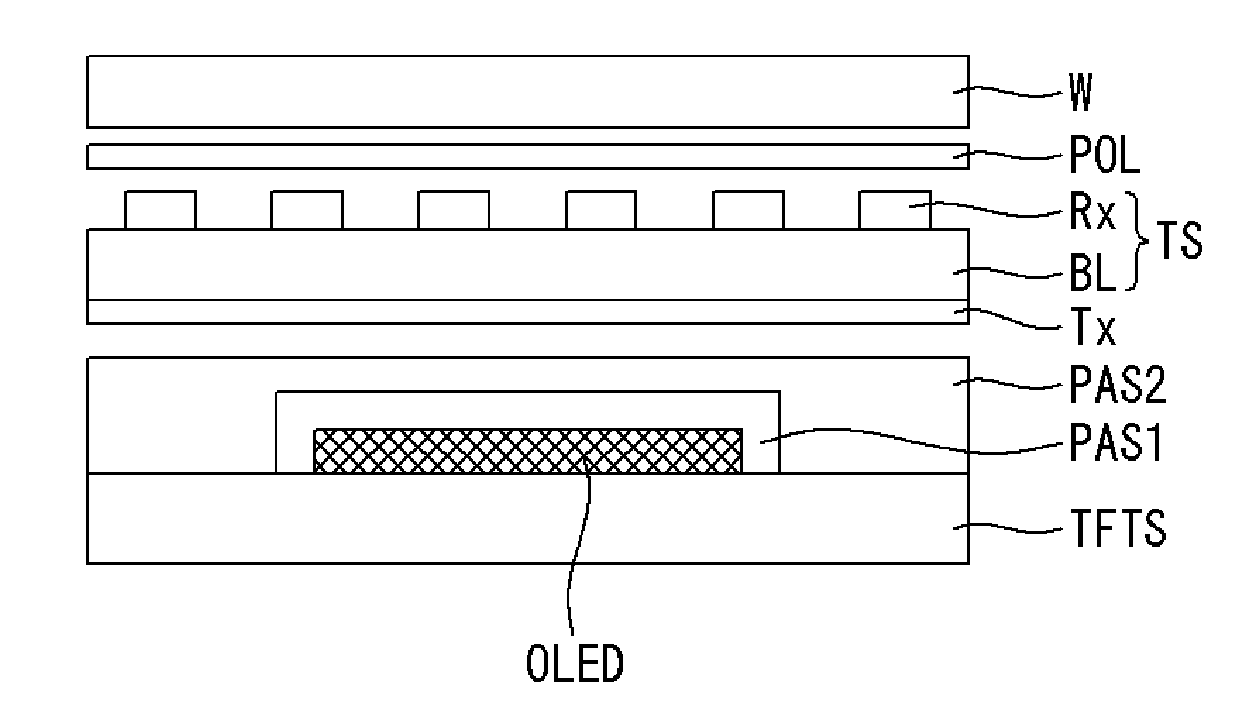
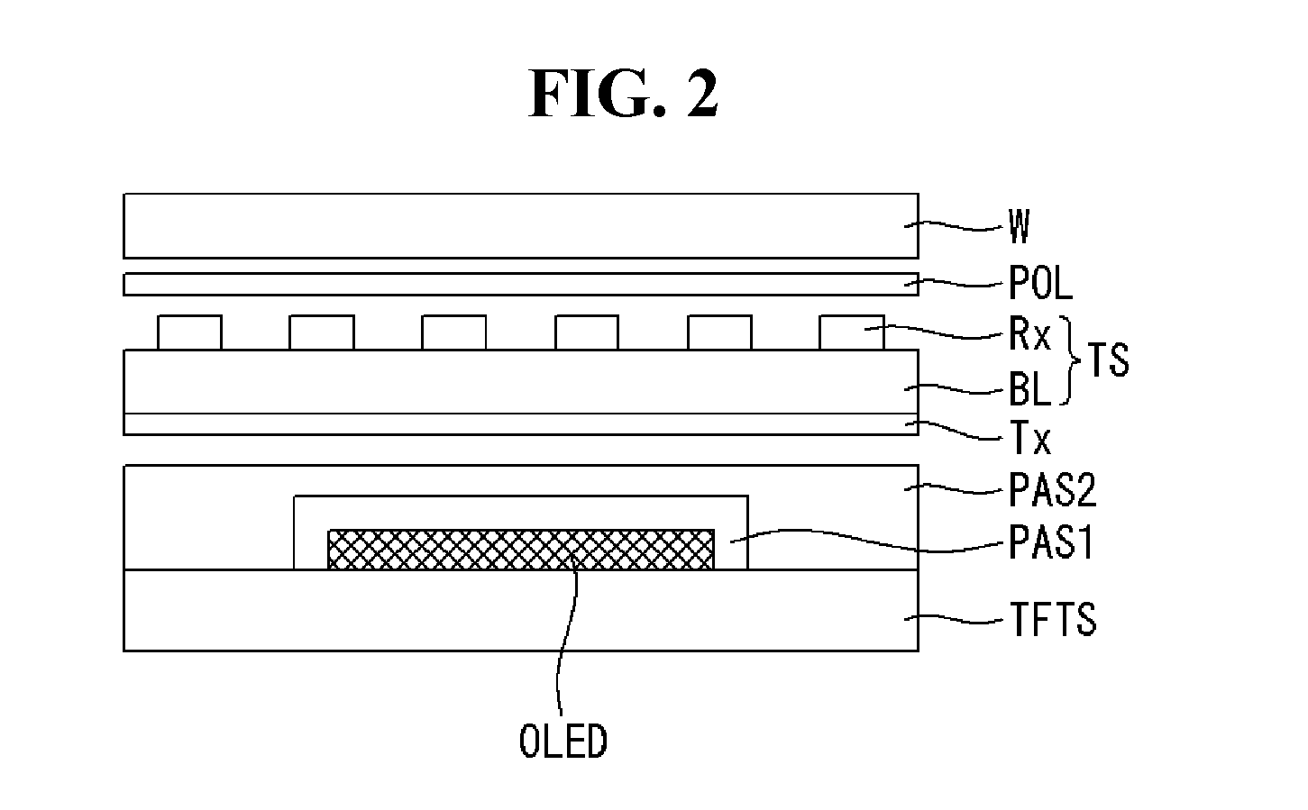
[0058]FIG. 2 is a cross-sectional view schematically illustrating a flexible OLED display device having a touch sensor according to one embodiment of this disclosure, FIG. 3 is a top planer view illustrating a touch sensor according to one embodiment of this disclosure shown in FIG. 2, FIG. 4A is a cross-sectional view taken along lines I-I′ and II-II′ of FIG. 3, and FIG. 4B is a cross-sectional view taken along line III-III′ of FIG. 3.

[0059]Referring to FIG. 2, the OLED display device according to one embodiment of this disclosure includes a thin film transistor (TFT) substrate TFT...


PUM


Abstract

An OLED display device having a touch sensor is provided. The touch sensor includes a base layer; a plurality of first touch electrodes arranged in a first direction on a first surface of the base layer; a plurality of second touch electrodes arranged in a second direction crossing the first direction on a second surface of the base layer; a plurality of first routing wires connected to the first touch electrodes on the first surface of the base layer, respectively; a plurality of second routing wires separated from the plurality of first routing wires and formed on the first surface of the base layer; and a plurality of third routing wires connected to the second routing wires respectively via holes, and formed on the second surface of the base layer. The base layer is one of a barrier layer, an anti-scratch layer, and a circular polarization layer.

Description

PRIORITY CLAIM[0001]This application claims the benefit of priority under 35 U.S.C. §119(a) to Korean Patent Application No. 10-2012-0138207 filed on Nov. 30, 2012, and Korean Patent Application No. 10-2013-0091068 filed on Jul. 31, 2013, the contents of each of which are incorporated by reference herein in their entirety.FIELD OF THE INVENTION[0002]This disclosure relates to a display device having a touch sensor and a method of manufacturing the same, more specifically an organic light emitting diode (OLED) display device capable of reducing cost as well as thickness and weight thereof and a method of manufacturing the same.DISCUSSION OF THE RELATED ART[0003]In recent years, liquid crystal display (LCD) devices and organic light emitting diode (OLED) display devices have become a mainstream in a flat display device market. In particular, the OLED display device has been gradually gaining popularity because it is a self light emitting element without requiring a backlight which is ...

Claims


Application Information

Patent Timeline
IPC IPC(8): H01L27/32H01L51/56
CPCG06F3/0412G06F3/0445G06F3/0446H10K59/40
Inventor LEE, NAMSEOKKOOK, YUNHOLEE, JUNGHWANYOO, TAEYEONHAN, YONGHEEHONG, SUNGGONCHOI, JINWOOK
Owner LG DISPLAY CO LTD
Why Eureka
Try Eureka