Multi-axis integrated MEMS devices with CMOS circuits and method therefor

a technology of integrated mems and circuits, applied in the field of integrated devices, can solve the problems of increasing the cost of mems development, focusing on mems development, and reducing the number of devices, so as to reduce the number of off-chip connections, facilitate use, and increase the device yield in dies

Active Publication Date: 2014-06-12
MOVELLA INC
View PDF6 Cites 16 Cited by
  • Summary
  • Abstract
  • Description
  • Claims
  • Application Information

AI Technical Summary

Benefits of technology

[0010]Many benefits are achieved by way of the one or more embodiments of the present invention over conventional techniques. For example, the present technique provides an easy to use process that relies upon conventional technology. In some embodiments, the method provides higher device yields in dies per wafer with the integrated approach. Also, the method provides a process and system that are compatible with conventional process technology without substantial modifications to conventional equipment and processes. This technique can reduce off-chip connections, which makes the mass production of smaller and thinner units possible. Additionally, integrated CMOS-MEMS technology can achieve high accuracy through the minimization of parasitic resistances and capacitances due to joint fabrication. Preferably, the invention provides for an improved integrated CMOS-MEMS device system and related applications for a variety of uses. Additionally, direct integration of CMOS and MEMS is especially desirable for systems implementing arrayed microsensors and microactuators on a single chip. This method can reduce off-chip connections, which makes the mass production of smaller and thinner units possible. Additionally, integrated CMOS-MEMS technology can achieve high accuracy through the minimization of parasitic resistances and capacitances due to joint fabrication.

Problems solved by technology

Although highly successful, ICs and in particular MEMS still have limitations.
Similar to IC development, MEMS development, which focuses on increasing performance, reducing size, and decreasing cost, continues to be challenging.
Additionally, applications of MEMS often require increasingly complex microsystems that desire greater computational power.
Unfortunately, such applications generally do not exist.

Method used


Image

  • Multi-axis integrated MEMS devices with CMOS circuits and method therefor
  • Multi-axis integrated MEMS devices with CMOS circuits and method therefor
  • Multi-axis integrated MEMS devices with CMOS circuits and method therefor

Examples


Embodiment Construction

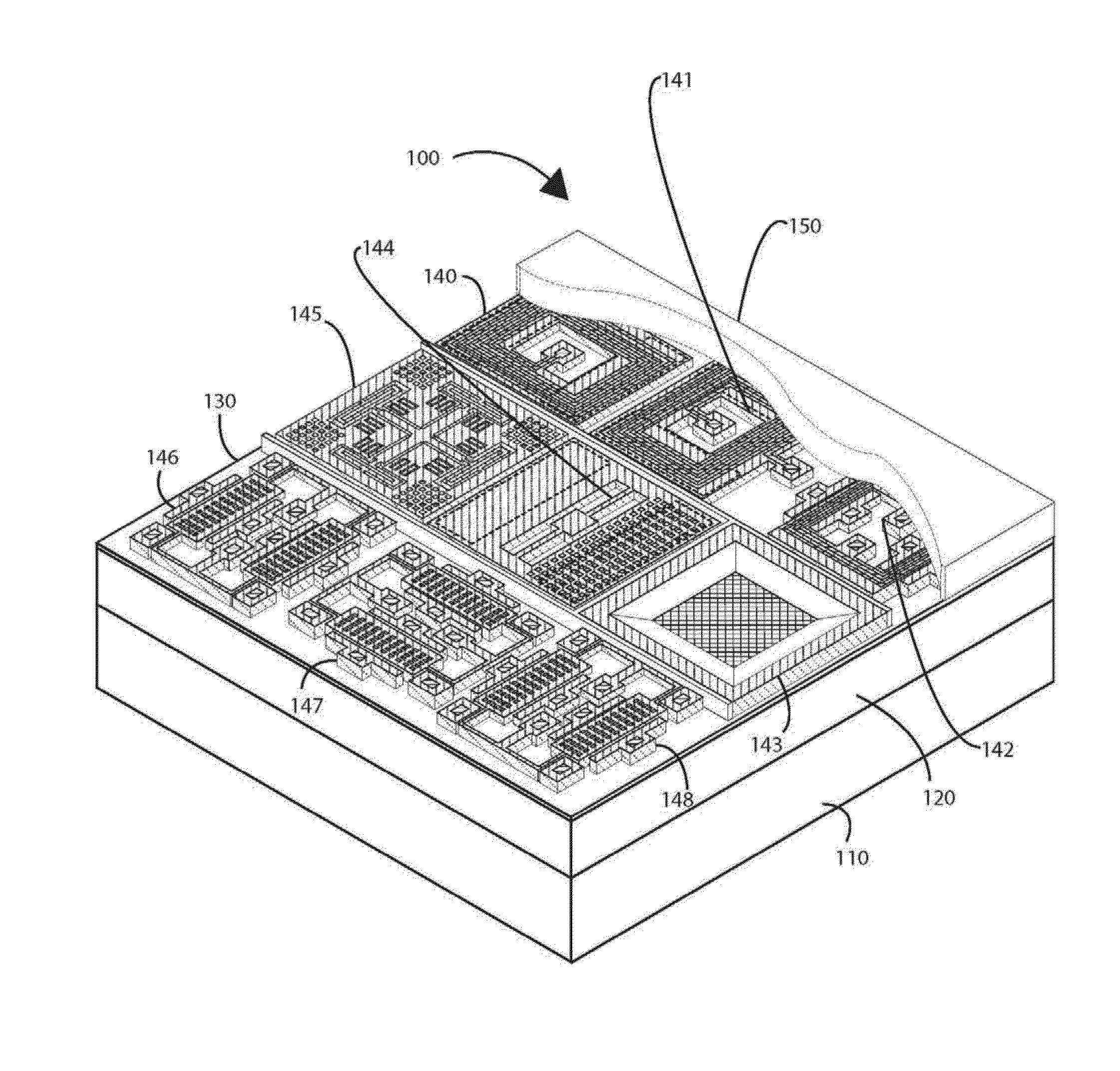
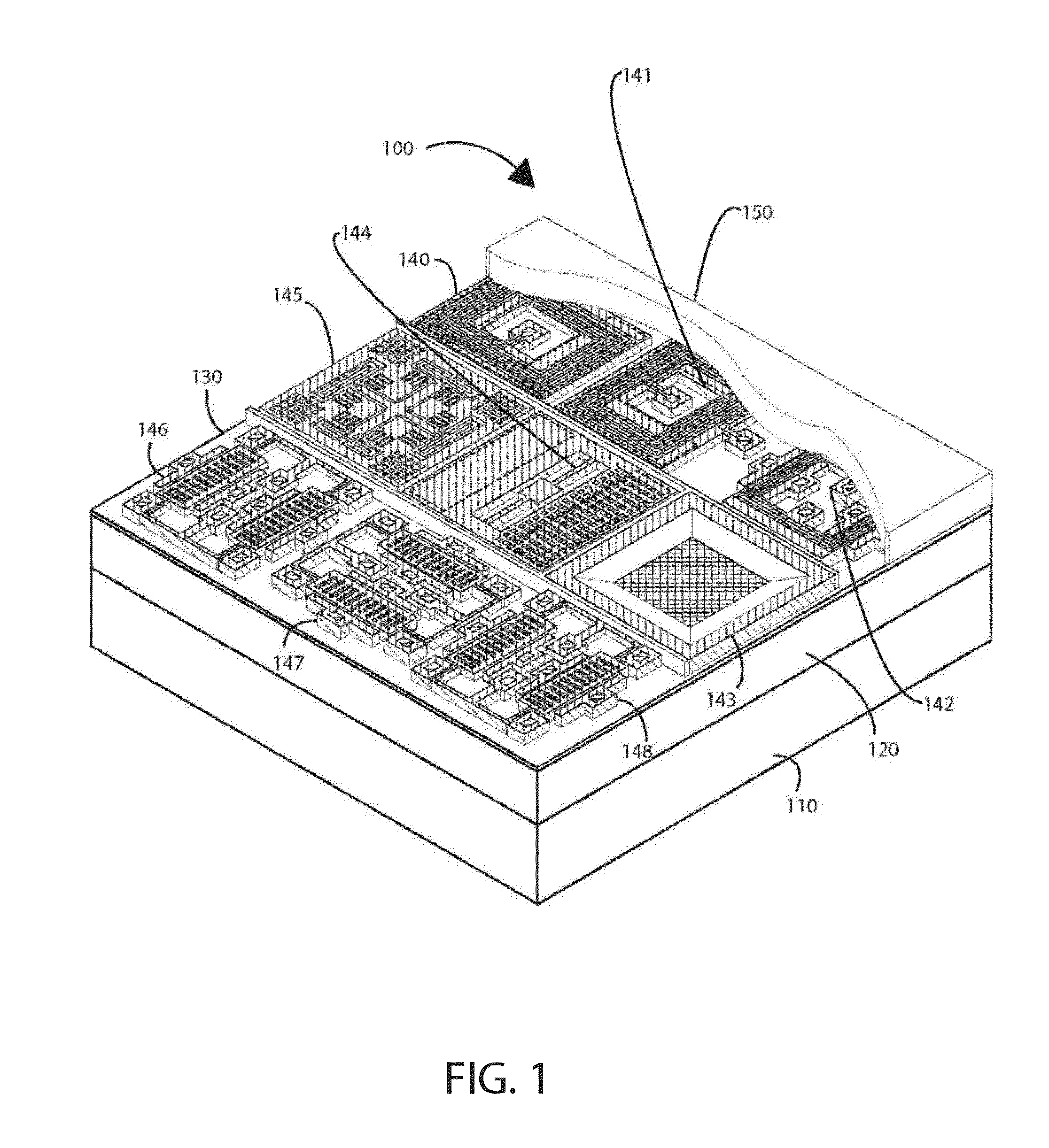
[0027]According to the present invention, techniques related generally to integrated devices and systems are provided. More particularly, embodiments of the present invention provide a system and method for integrating MEMS devices with other system applications configured on at least CMOS integrated circuit devices. Merely by way of example, the MEMS devices can include at least an accelerometer, a gyroscope, a magnetic field sensor, a pressure sensor, a microphone, a humidity sensor, a temperature sensor, a chemical sensor, a biosensor, an inertial sensor, and others. Additionally, the other applications include at least a sensor application or applications, system applications, and broadband applications, among others. But it will be recognized that the invention has a much broader range of applicability.

[0028]FIG. 1 is a simplified perspective diagram of an integrated multi-axial mechanical device and integrated circuit system according to an embodiment of the present invention....


PUM

PropertyMeasurementUnit
thicknessaaaaaaaaaa
widthaaaaaaaaaa
widthaaaaaaaaaa

Abstract

An integrated multi-axis mechanical device and integrated circuit system. The integrated system can include a silicon substrate layer, a CMOS device region, four or more mechanical devices, and a wafer level packaging (WLP) layer. The CMOS layer can form an interface region, on which any number of CMOS and mechanical devices can be configured. The mechanical devices can include MEMS devices configured for multiple axes or for at least a first direction. The CMOS layer can be deposited on the silicon substrate and can include any number of metal layers and can be provided on any type of design rule. The integrated MEMS devices can include, but not exclusively, any combination of the following types of sensors: magnetic, pressure, humidity, temperature, chemical, biological, or inertial. Furthermore, the overlying WLP layer can be configured to hermetically seal any number of these integrated devices.

Description

CROSS-REFERENCES TO RELATED APPLICATIONS[0001]The present application is a divisional application of U.S. patent application Ser. No. 12 / 983,309, filed Jan. 2, 2011, which claims priority to Provisional Patent Application No. 61 / 292,141, filed Jan. 4, 2010, both of which are incorporated herein by reference for all purposes. The present invention also incorporates by reference, for all purposes, the following pending patent applications related to sensor and MEMS devices: U.S. patent application Ser. No. 12 / 913,440, filed Oct. 29, 2010, U.S. patent application Ser. No. 12 / 859,631, filed Aug. 19, 2010, U.S. Pat. App. No. 61 / 356,467, filed Jun. 18, 2010, U.S. patent application Ser. No. 12 / 859,672, filed Aug. 19, 2010, and U.S. patent application Ser. No. 12 / 859,647, filed Aug. 19, 2010.BACKGROUND OF THE INVENTION[0002]Embodiments of the present invention relates generally to integrated devices. More particularly, embodiments of the present invention provide a system and method for in...

Claims


Application Information

Patent Timeline
Patent Type & Authority Applications(United States)
IPC IPC(8): B81C1/00
CPCH01L27/0688H01L27/14603B81C2203/0771B81B7/02B81C1/00246H01L2224/48091H01L2924/16235H01L2924/00014B81C1/0023
Inventor YANG, XIAO "CHARLES"
Owner MOVELLA INC
Why Eureka
Try Eureka