Apparatus and Method For High Voltage I/O Electro-Static Discharge Protection

a technology of electro-static discharge and apparatus, applied in the direction of semiconductor electrostatic transducers, emergency protective arrangements for limiting excess voltage/current, microphone structural associations, etc., can solve the problem that the metal oxide semiconductor devices are quite sensitive to electro-static discharge damage, fail to adequately address the problem, and the problem is particularly sever

Active Publication Date: 2014-06-26
KNOWLES ELECTRONICS INC
View PDF10 Cites 39 Cited by
  • Summary
  • Abstract
  • Description
  • Claims
  • Application Information

AI Technical Summary

Problems solved by technology

Metal Oxide Semiconductor (MOS) devices are quite sensitive to Electro-Static Discharge (ESD) damage.
The problem is especially pronounced in deep submicron Complementary Metal Oxide Semiconductor (CMOS) processes because the gate oxide of the transistors is just few nano-meters thick.
Unfortunately, previous attempts at solving the ESD discharge problem using this circuitry have shortcomings and have failed to adequately address the problem.

Method used


Image

  • Apparatus and Method For High Voltage I/O Electro-Static Discharge Protection
  • Apparatus and Method For High Voltage I/O Electro-Static Discharge Protection
  • Apparatus and Method For High Voltage I/O Electro-Static Discharge Protection

Examples


Embodiment Construction

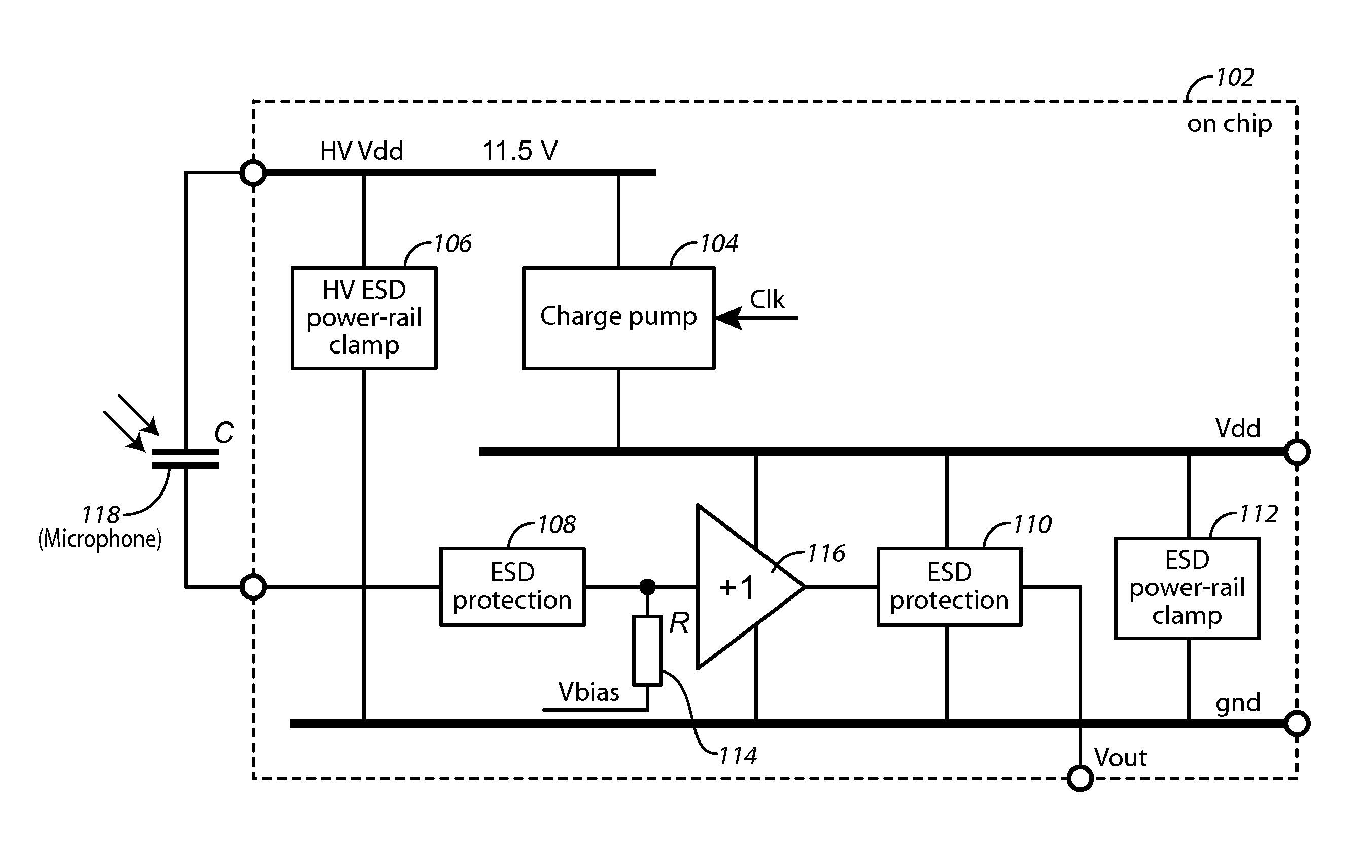
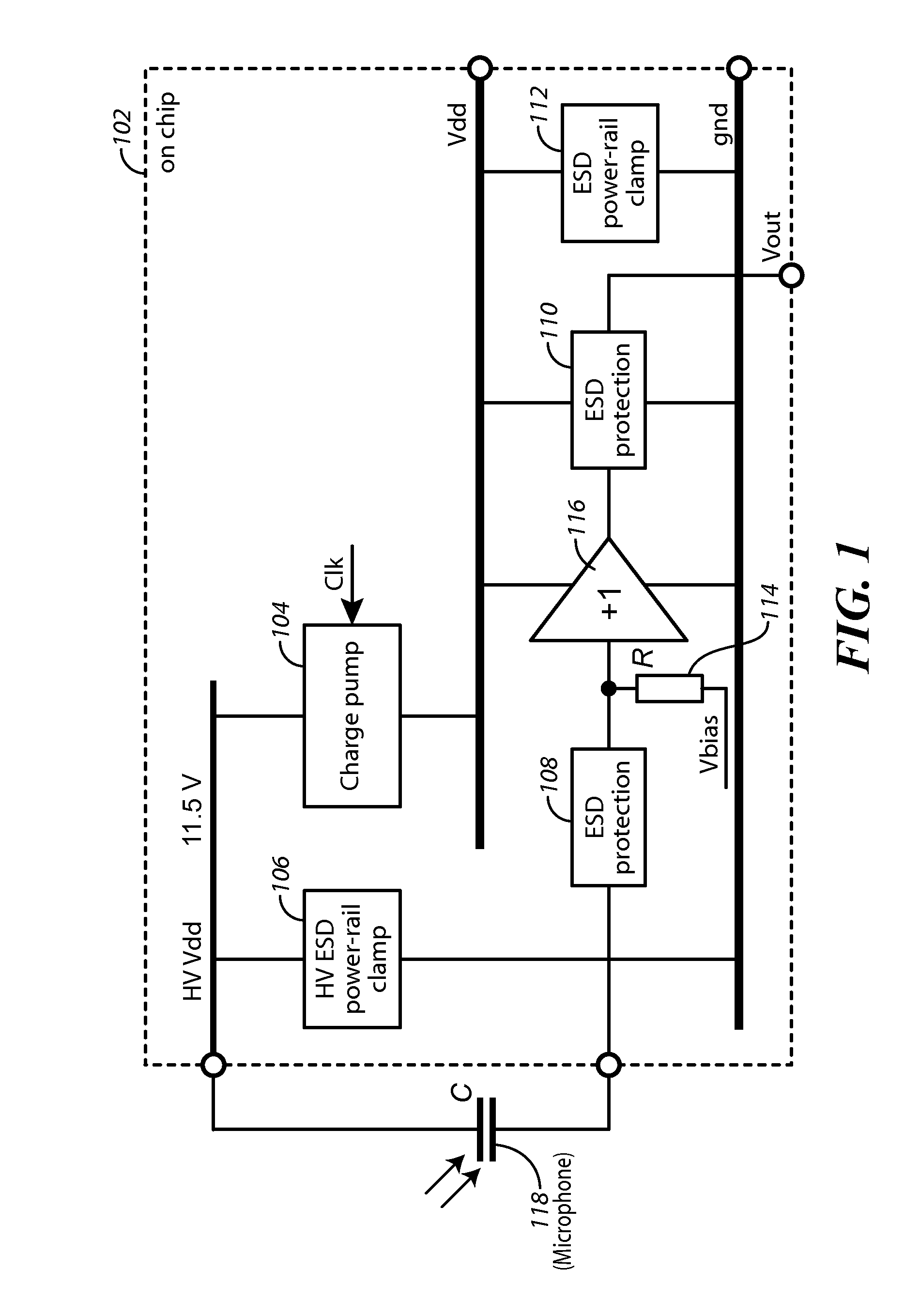
[0017]Approaches are provided herein for a high voltage ESD power-rail clamp to be used with or at a charge pump output. ESD protection approaches for the high voltage terminal of a MEMS microphone can be implemented in a standard low voltage CMOS process. By “process” and as used herein, it is meant the construction process.

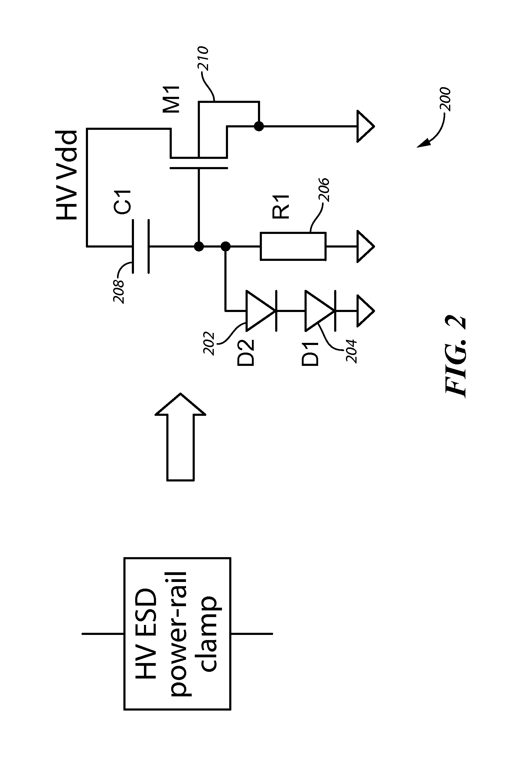
[0018]In some aspects of the present approaches, the output of a charge pump can withstand high ESD voltages. Consequently, high voltage ESD power rail clamps can be implemented with stacked standard low voltage transistors. In one example, the high voltage operation of the high voltage ESD power rail clamps is achieved by forming high voltage NWELL / DNWELL regions of the PMOS and NMOS transistors used to construct the high voltage ESD power rail clamps. In this way, the NWELL / DNWELL to substrate breakdown voltage is increased from about 10 V to 45 V in a standard 0.18 CMOS process. As a result, the need for an expensive high voltage process to construct these de...


PUM


Abstract

An electronics chip includes a charge pump and at least one high voltage (HV) electro-static discharge (ESD) module. The charge pump is configured to provide a predetermined voltage across a microphone. The devices described herein are implemented in a standard low voltage CMOS process and has a circuit topology that provides an inherent ESD protection level (when it is powered down), which is higher than the operational (predetermined) DC level. At least one high voltage (HV) electro-static discharge (ESD) module is coupled to the output of the charge pump. The HV ESD module is configured to provide ESD protection for the charge pump and a microelectromechanical system (MEMS) microphone that is coupled to the chip. The at least one HV ESD module includes a plurality of PMOS or NMOS transistors having at least one high voltage NWELL / DNWELL region formed within selected ones of the PMOS or NMOS transistors. The at least one high voltage NWELL / DNWELL region has a breakdown voltage sufficient to allow a low voltage process to be used to construct the chip and still allow the HV ESD module to provide ESD protection for the chip.

Description

CROSS-REFERENCE TO RELATED APPLICATION[0001]This patent claims benefit under 35 U.S.C. §119 (e) to U.S. Provisional application No. 61 / 739,284, filed Dec. 19, 2012 and entitled “Apparatus and Method for High Voltage I / O Electrostatic Discharge Protection in Standard Low Voltage CMOS Process,” the contents of which are incorporated herein by reference in their entirety.TECHNICAL FIELD[0002]This application relates to electrostatic discharge (ESD) protection of high voltage I / O in microphone circuits.BACKGROUND OF THE INVENTION[0003]The condenser microphone is a widely used type of microphone. In some respects, this microphone can be considered a variable capacitor whose capacitive value is modulated by the pressure of an incoming sound wave. In this view, one of the capacitor plates is static, while the other one is mobile (i.e., the moving diaphragm component). The sound wave changes the distance between the plates, and this respectively changes the capacitance of the representative...

Claims


Application Information

Patent Timeline
Patent Type & Authority Applications(United States)
IPC IPC(8): H02H9/04
CPCH02H9/04H01L27/0248H02H9/046H04R19/04H04R19/005B81B3/0027B81B2201/0257H01L27/0266H01L29/7816H02M3/07H04R1/04H04R2201/003
Inventor GUEORGUIEV, SVETOSLAV RADOSLAVOVFURST, CLAUS ERDMANNJOERGENSEN, TORE SEJR
Owner KNOWLES ELECTRONICS INC
Why Eureka
Try Eureka