Method for manufacturing wiring board

a manufacturing method and technology for wiring boards, applied in the manufacture of printed circuits, solid-state devices, basic electric elements, etc., can solve the problems of reducing the fabrication yield of wiring boards, affecting the quality of wiring boards, and difficulty in thinning the entire thickness of wiring boards, etc., to achieve high producibility

Active Publication Date: 2014-07-03
KYOCERA CORP
View PDF14 Cites 12 Cited by
  • Summary
  • Abstract
  • Description
  • Claims
  • Application Information

AI Technical Summary

Benefits of technology

[0010]In the method for manufacturing the wiring board of the present invention, the separable metal foil which is composed of the first metal foil and the second metal foil that are separably adhered to each other and whose area is larger than the area of the product forming region and is smaller than the area of the supporting substrate is pressurized against the upper surface of the product forming region so that the first metal foil faces the supporting substrate and is buried into the supporting substrate, and the lower surface and

Problems solved by technology

For this reason, it is difficult to thin the entire thickness of wiring boards.
When the plating medical solution infiltrates in such a manner, adhesion between the carrier copper foil and the ultrathin copper foil is weakened

Method used


Image

  • Method for manufacturing wiring board
  • Method for manufacturing wiring board
  • Method for manufacturing wiring board

Examples


Embodiment Construction

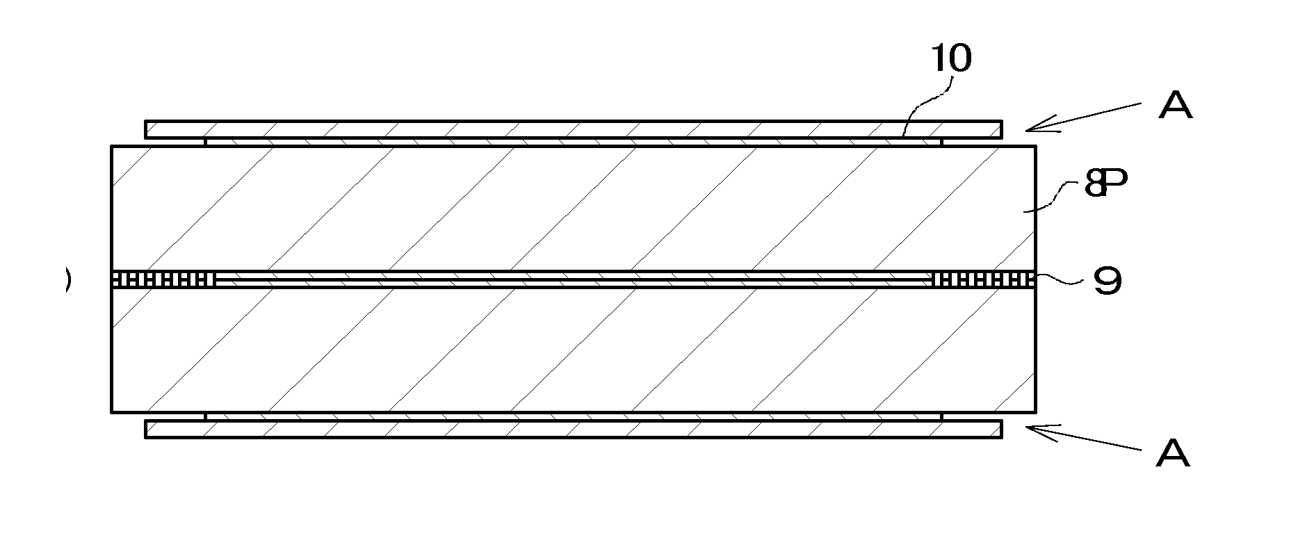
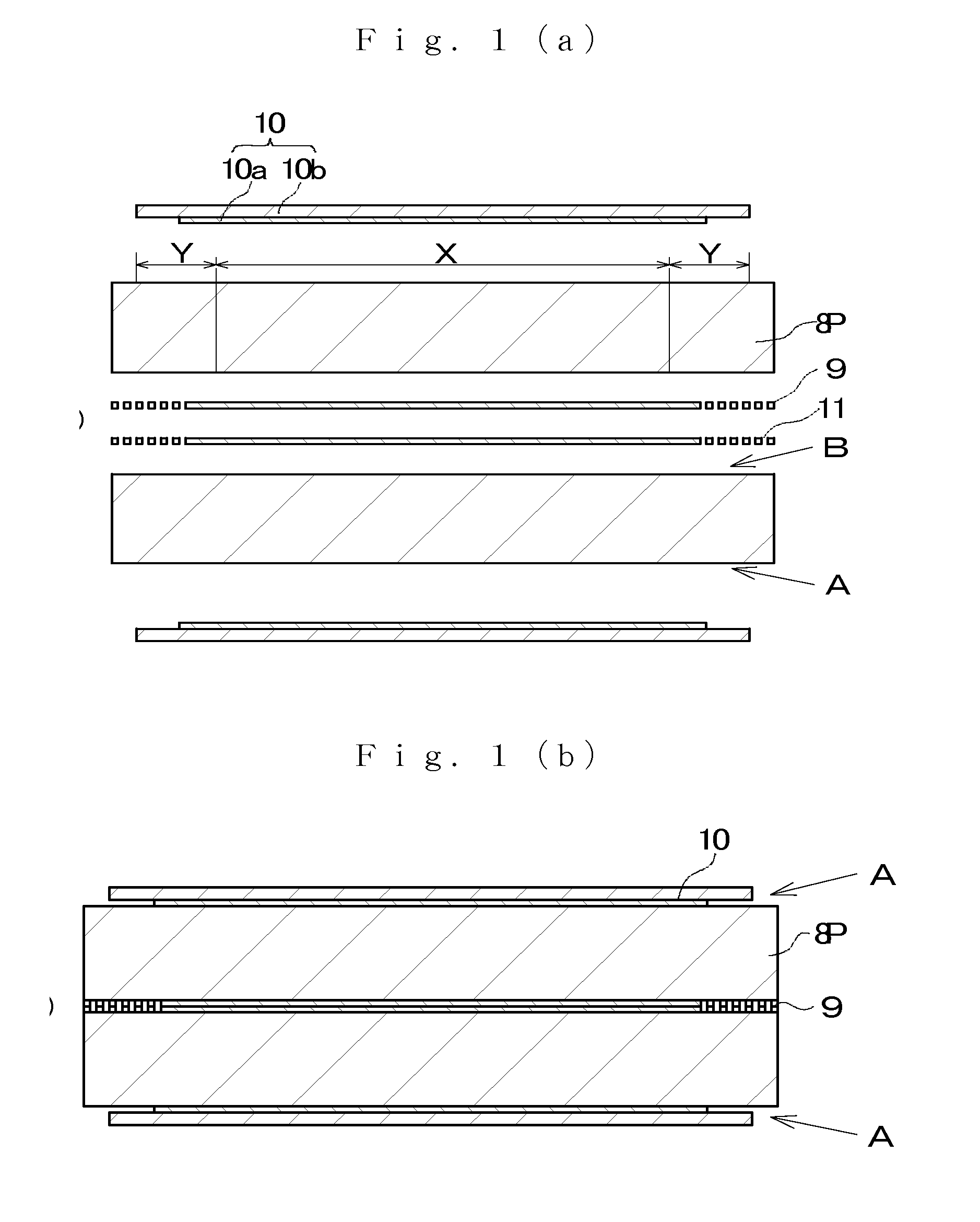
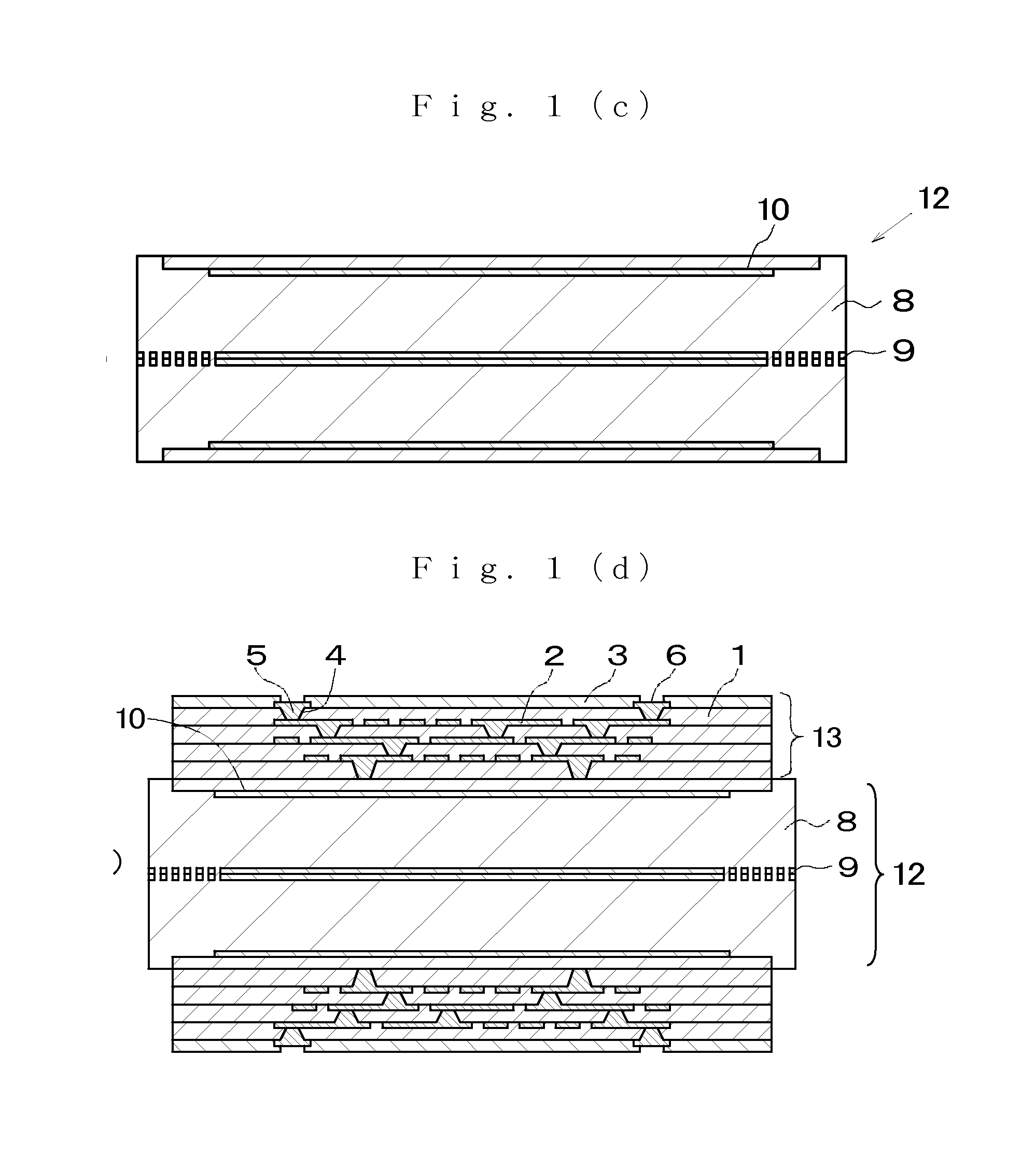
[0015]A method for manufacturing a wiring board according to one embodiment of the present invention is described with reference to FIGS. 1A to 1J. As illustrated in FIG. 1A, two prepregs 8P, two separation films 9, and two separable metal foils 10 are prepared.

[0016]When a laminated body 14 for a wiring board 20, described later, is manufactured, the prepregs 8P are used for forming a supporting substrate 8 for supporting the laminated body 14 with necessary flatness being maintained. One main surface A of the prepreg 8P is a product forming surface, and the other main surface B is a separation surface. Each of the prepregs 8P has a product forming region X, and a marginal region Y on an outer periphery of the product forming region X. The product forming region X is a square region, and the wiring board 20 is formed on the product forming region X. For convenience, FIG. 1 illustrates only one product forming region X corresponding to one wiring board 20, but actually the supportin...


PUM

PropertyMeasurementUnit
Lengthaaaaaaaaaa
Thicknessaaaaaaaaaa
Thicknessaaaaaaaaaa

Abstract

A method for manufacturing a wiring board according to the present invention includes the steps of preparing a supporting substrate having a product forming region and a marginal region; preparing a separable metal foil whose area is larger than that of the product forming region and is smaller than that of the supporting substrate; fixing the separable metal foil to the supporting substrate by burying into the supporting substrate; forming a build-up section on the buried separable metal foil; integrally cutting out the supporting substrate, the separable metal foil and the build-up section; obtaining a laminated body for wiring board composed of the second metal foil and the build-up section by separating the first metal foil and the second metal foil; and forming the wiring conductor layer by removing a part of the second metal foil.

Description

BACKGROUND OF THE INVENTION[0001]1. Field of the Invention[0002]The present invention relates to a method for manufacturing a wiring board used for mounting a semiconductor element such as a microchip.[0003]2. Description of Related Art[0004]In recent years, amid the advance in a high performance and thinning of electronic devices such as portable video game players and communication devices, build-up wiring boards are present as high-density wiring boards used for these devices. General build-up wiring boards have a configuration such that insulating layers and wiring conductors are alternately laminated on both surfaces of a core substrate having a thickness of about 0.2 to 2.0 mm. Core substrates are formed by a resin substrate and a wiring conductor. The resin substrate is obtained by impregnating an electric insulating material such as epoxy resin in a glass fiber. The wiring conductor is made of a copper foil. The insulating layer is formed of resin having a thickness of about...

Claims


Application Information

Patent Timeline
IPC IPC(8): H05K3/04
CPCH05K3/04H01L21/6835H01L23/49822H01L2221/68318H01L2221/68345H01L2221/68381H01L2224/16225H05K3/0097H05K3/4682Y10T29/49156H05K3/46
Inventor NARUMI, DAISUKENAKATOMI, YOSHINORIYASUDA, MASAHARU
Owner KYOCERA CORP
Why Eureka
Try Eureka