Display device with binary mode amoled pixel pattern

a display device and amoled pixel technology, applied in the field of display devices, can solve the problems of wasting a significant amount of valuable power, consuming 40-60% of the power supplied by tft transistors in amoled display devices, and complicating the circuit design of timing control logic, so as to reduce the power consumed by transistors and increase the power consumption efficiency of display devices. , the timing control logic of such a device can be simplified, the effect of reducing the power consumption o

Inactive Publication Date: 2014-07-03
NVIDIA CORP
View PDF5 Cites 16 Cited by
  • Summary
  • Abstract
  • Description
  • Claims
  • Application Information

AI Technical Summary

Benefits of technology

[0006]Therefore, it would be advantageous to reduce the power consumed by the transistors in an AMOLED display device and thereby increase power consumption efficiency of the display device. It would also be advantageous if the timing control logic for such a device can be simplified. Moreover, it would be also advantageous to be capable of adjusting the global luminance of a display panel in response to ambient light level.
[0007]Accordingly, embodiments of the present disclosure provide a mechanism to reduce power consumption by using transistors operating in a binary on / off mode to drive an array of OLEDs. The mechanism also allows for simplified designs of timing control logic and global luminance control of the display device. Embodiments of the present disclosure advantageously include an AMOLED layer with each color element comprising a discrete array of OLED junctions coupled to a plurality of transistors. Thus, luminance of the color element can be digitally controlled by turning on a selected combination of the transistors and thereby activating luminance of the associated OLED junctions. The plurality of OLED junctions of a respective color element vary in size in accordance with the value of the binary digit to which they are controlled. In one embodiment, the plurality of junctions that make up a color element may vary in size according to 2n, where n is the junction number and may correspond to a bit position of a control color bit that that controls the junction. The color bit is located within a color byte for controlling the entire color element.

Problems solved by technology

Since the second transistor operates in its linear region, a considerable fraction of the power can be consumed by the internal resistance of the second transistor which wastes a significant amount of valuable power, especially when used in a mobile computing device fitted with a limited size battery.
For example, the TFT transistors in an AMOLED display device may consume 40-60% of the power supplied to drive the AMOLED display device.
Further, in a conventional design, since luminance of each OLED is driven by a continuous current through an associated transistor, the binary color values, e.g. in the format of a 8:8:8 byte, usually have to be converted to analog data through a Digital-Analog-Converter (DAC) in a timing controller, which complicates the circuit design in the timing control logic.
Although setting the display panel luminance constantly at its maximum level would ensure the images are visible in the widest range of ambient light levels, the unnecessarily brightness increases power consumption, and shortens operating lifetime of the display panel.
Also, excessive contrast between the displayed images and dark ambient environments may cause eye discomforts.

Method used


Image

  • Display device with binary mode amoled pixel pattern
  • Display device with binary mode amoled pixel pattern
  • Display device with binary mode amoled pixel pattern

Examples


Embodiment Construction

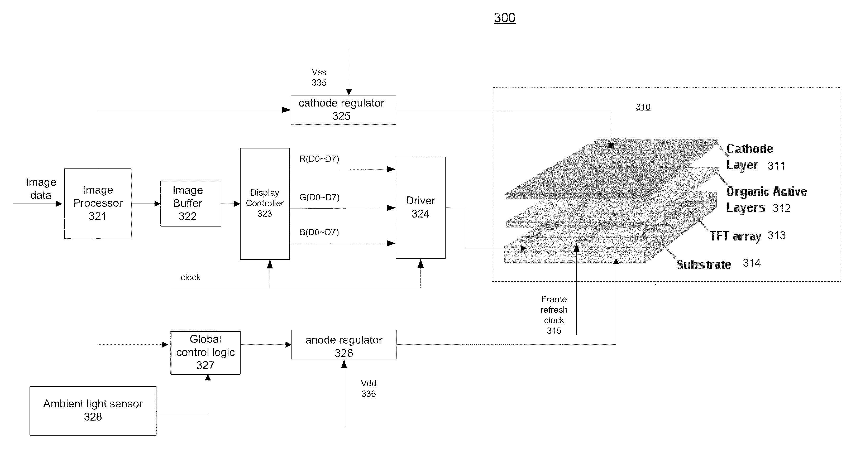
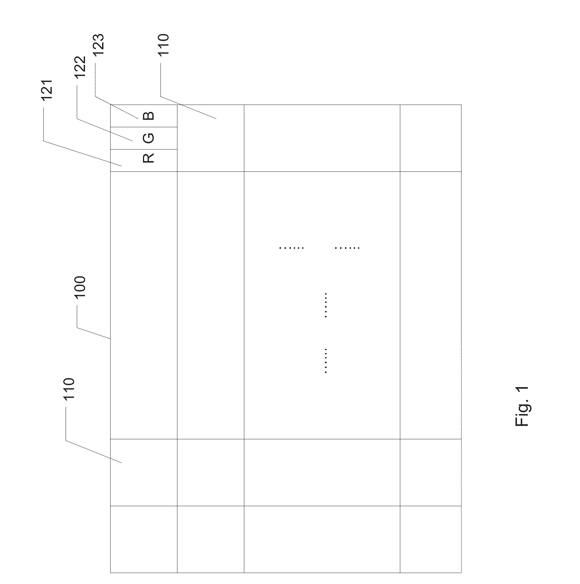
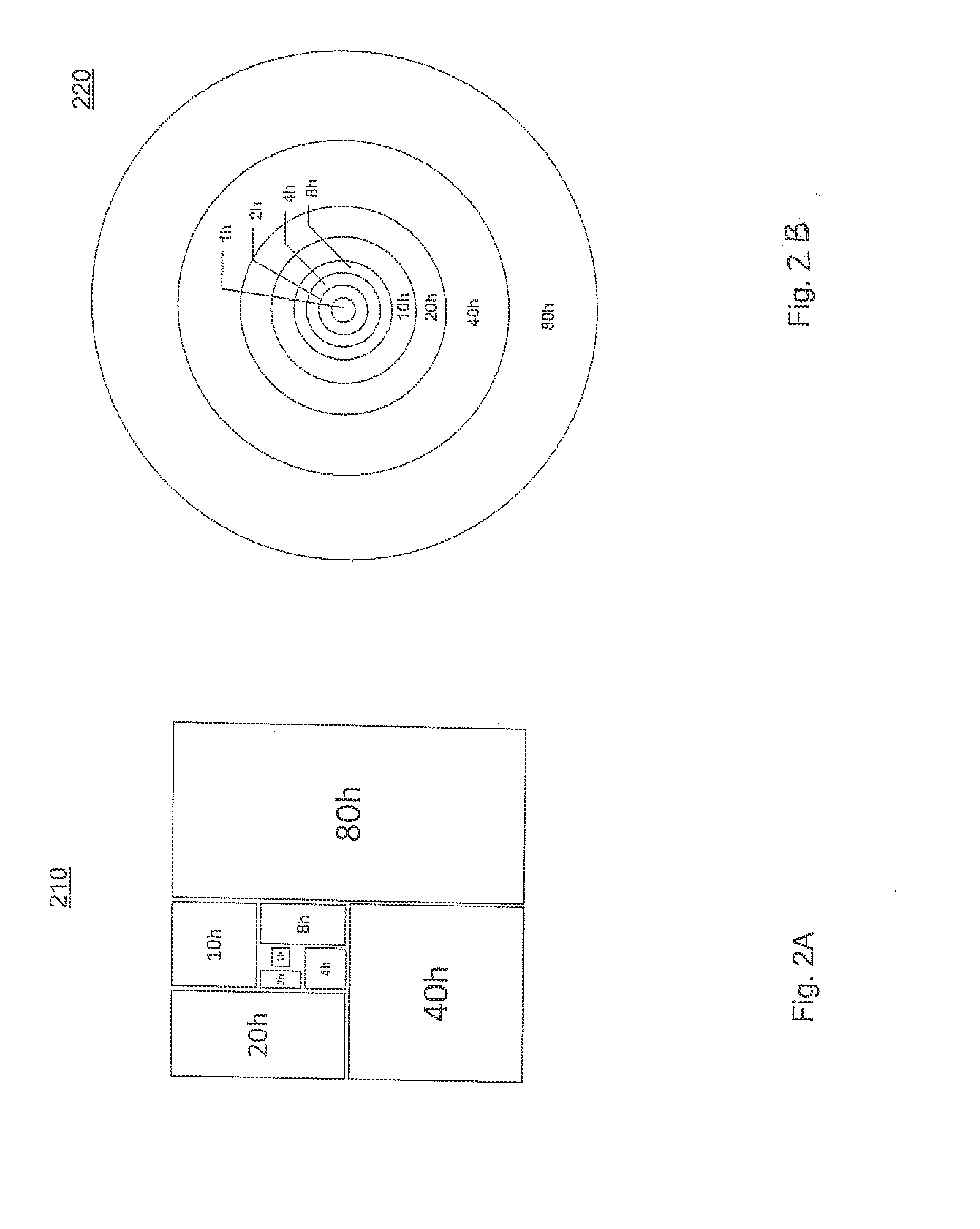
[0021]Reference will now be made in detail to the preferred embodiments of the present invention, examples of which are illustrated in the accompanying drawings. While the invention will be described in conjunction with the preferred embodiments, it will be understood that they are not intended to limit the invention to these embodiments. On the contrary, the invention is intended to cover alternatives, modifications and equivalents, which may be included within the spirit and scope of the invention as defined by the appended claims. Furthermore, in the following detailed description of embodiments of the present invention, numerous specific details are set forth in order to provide a thorough understanding of the present invention. However, it will be recognized by one of ordinary skill in the art that the present invention may be practiced without these specific details. In other instances, well-known methods, procedures, components, and circuits have not been described in detail ...


PUM


Abstract

An AMOLED display panel comprising a plurality of color elements in each pixel with each of the color elements comprising a discrete plurality of illuminating units associated with a plurality of transistors operating in a binary mode. The plurality of illuminating units have different sizes in accordance with 2n size, where n is the illuminating unit's number. n may also be the bit position of the bit line that controls the illuminating unit. The collective luminance of each color element can be digitally controlled by selectively activating a combination of the discrete illuminating units to their nominal luminance. The discrete plurality of illuminating units in each pixel may be directly controlled by RGB pixel data without the requirement for digital analog conversion.

Description

TECHNICAL FIELD[0001]The present disclosure relates generally to the field of display devices and more specifically to the field of light-emitting diode display panels.BACKGROUND[0002]An Organic Light-Emitting Diode (OLED) display consists of a matrix of Organic Light-Emitting Diode (OLED) pixels that generate light upon electrical activation. Conventionally, luminance of each OLED increases with more current flowing to it. Typically, this continuous current flow is controlled by at least two transistors at each pixel, one to start or stop the charging of a storage capacitor and the second to provide a voltage source at the level needed to create a constant current to the pixel. In a commonly adopted RGB color model, each light emitting element, i.e., pixel, comprises a red (R) OLED element, a green (G) OLED element, and a blue (B) OLED element for emitting red color, green color and blue color light, respectively. A pixel can express a desired color in a certain frame by mixing lig...

Claims


Application Information

Patent Timeline
Patent Type & Authority Applications(United States)
IPC IPC(8): G09G3/32
CPCG09G3/3233G09G3/3225G09G3/2074G09G2300/0828
Inventor XU, SHUANG
Owner NVIDIA CORP
Why Eureka
Try Eureka