Semiconductor integrated circuit design supporting apparatus, method, and program

a technology of integrated circuit design and supporting apparatus, applied in the direction of computer aided design, program control, instruments, etc., can solve the problems of large amount of time and large scale in rtl design, and achieve the effect of small circuit scale hardware configuration and short period of tim

Active Publication Date: 2014-07-03
MITSUBISHI ELECTRIC CORP
View PDF1 Cites 7 Cited by
  • Summary
  • Abstract
  • Description
  • Claims
  • Application Information

AI Technical Summary

Benefits of technology

[0019]In the semiconductor integrated circuit design supporting apparatus according to one embodiment of the present invention, the necessary delay that is required to be inserted between the modules is acquired based on the latency value of each module acquired from the HDL or the synthetic log obtained through the high level synthesis. Further, the pin having an input that receives the FF is extracted from the HDL or the synthetic log obtained through the high level synthesis, to thereby acquire the number of stages of FF reception, that is, the input delay. Then, the latency re-adjusting means obtains the optimum delay based on the necessary delay and the input delay. Then, ba

Problems solved by technology

In recent years, integrated circuits have become larger in scale, which has caused a problem in that a large amount of time is required in RTL design.
Therefore, there ari

Method used


Image

  • Semiconductor integrated circuit design supporting apparatus, method, and program
  • Semiconductor integrated circuit design supporting apparatus, method, and program
  • Semiconductor integrated circuit design supporting apparatus, method, and program

Examples


first embodiment

[0060]A semiconductor integrated circuit design supporting apparatus according to one embodiment of the present invention includes a computer main body, a graphic display device, a keyboard, a mouse, a compact disc read-only memory (CD-ROM) device to which a CD-ROM is mounted, and a network.

[0061]A semiconductor integrated circuit design supporting program is supplied by means of a storage medium such as a CD-ROM, and is executed by the computer main body. An operator operates the keyboard or the mouse while looking at the graphic display device so as to control the semiconductor integrated circuit design supporting program to support design of a semiconductor integrated circuit.

[0062]Further, the semiconductor integrated circuit design supporting program may be supplied to the computer main body via the network from another computer through a communication line.

[0063]The computer main body includes a central processor unit (CPU), a read-only memory (ROM), a random access memory (RA...

second embodiment

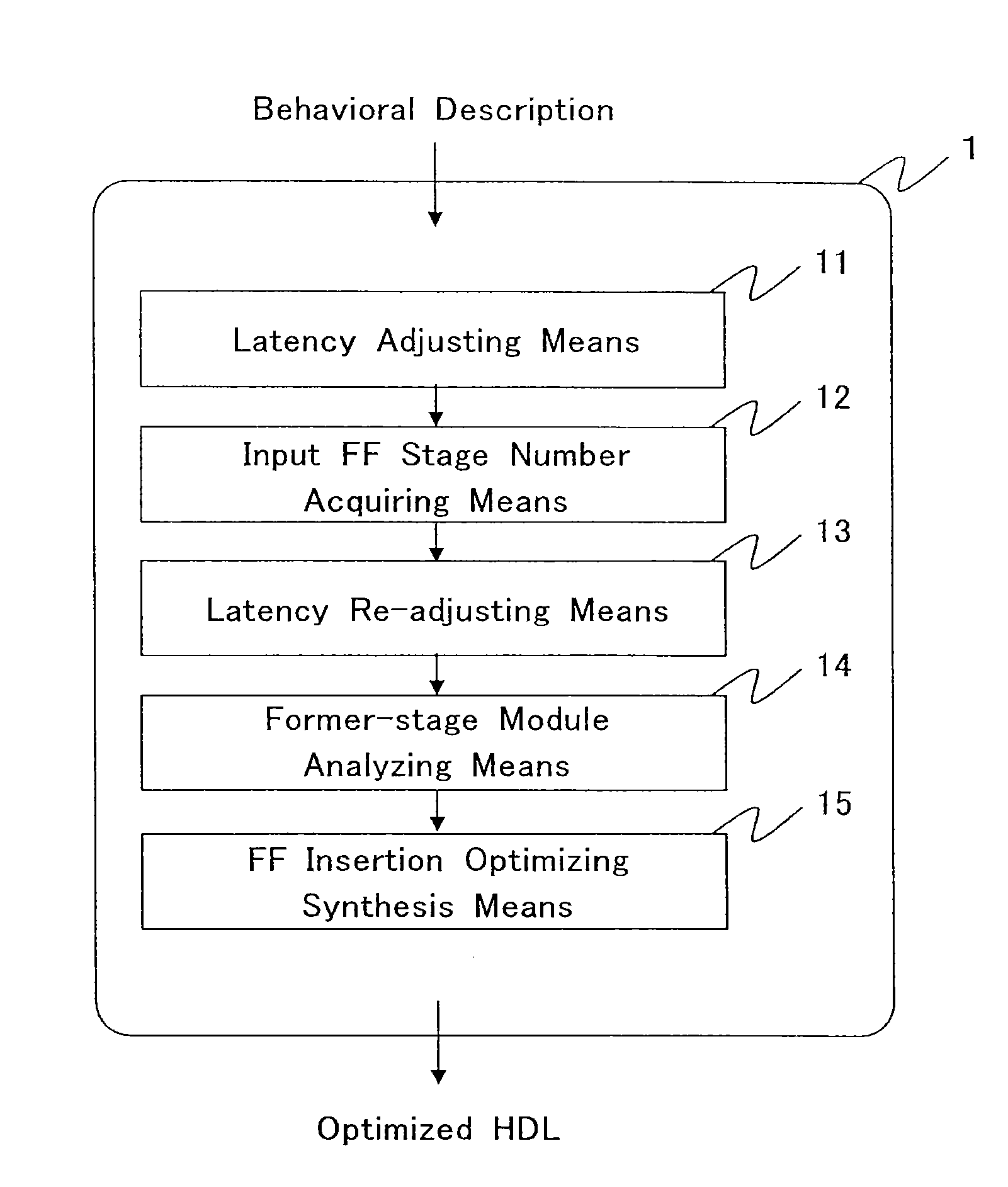
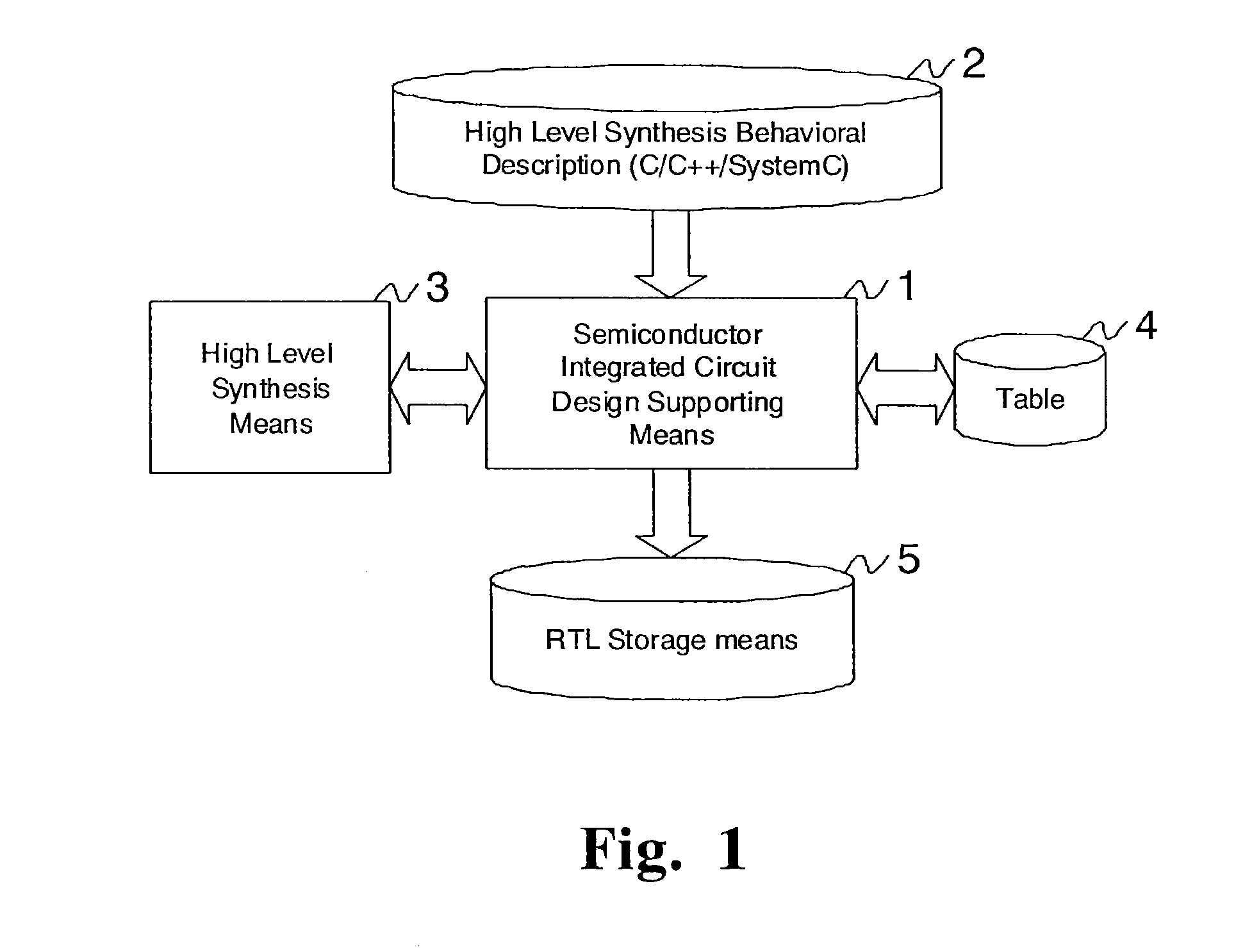
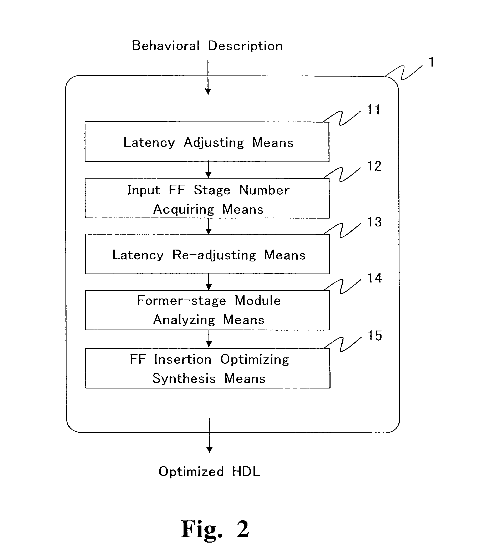
[0078]Next, a semiconductor integrated circuit design supporting apparatus according to a second embodiment of the present invention is described. The configuration of the semiconductor integrated circuit design supporting apparatus according to the second embodiment of the present invention is the same as that in FIG. 1.

[0079]The semiconductor integrated circuit design supporting means 1 illustrated in FIG. 1 inputs a behavioral description code (hereinafter simply referred to as “behavioral description”) of an integrated circuit, which is written in high level language (such as C language, C++ language, and SystemC language) from the high level synthesis behavioral description storing means 2. Then, in cooperation with the high level synthesis means 3 that executes high level synthesis of analyzing the behavioral description to generate an RTL description, the semiconductor integrated circuit design supporting means 1 generates the RTL description and outputs the RTL description t...


PUM


Abstract

A latency adjusting part calculates a necessary delay based on the number of FFs that are required to be inserted between respective modules through high level synthesis of a behavioral description. An input FF stage number acquiring part extracts a pin having an input that receives an FF, and acquires the number of stages of input FFs of FF reception. A latency re-adjusting part obtains an optimum delay based on the above-mentioned necessary delay and input delay. A former-stage module analyzing part detects, based on the above-mentioned synthetic log or HDL, a state having a minimum total number of FFs. An FF insertion optimizing synthesis part subjects an entire circuit to high level synthesis again based on the above-mentioned optimum delay and an FF inserting position obtained based on the state having the minimum number of FFs, to thereby obtain optimized HDL.

Description

BACKGROUND OF THE INVENTION[0001]1. Field of the Invention[0002]The present invention relates to a semiconductor integrated circuit design supporting apparatus, method, and program for supporting design of a semiconductor integrated circuit, which utilizes high level synthesis or behavioral synthesis of automatically generating, based on a behavioral description of a circuit, a register transfer level (RTL) description for the semiconductor integrated circuit.[0003]2. Description of the Related Art[0004]Hitherto, a semiconductor integrated circuit has been designed with use of hardware description language (HDL) by RTL, which describes the behavior of combinational logic between registers (flip-flops) included in a circuit. In recent years, integrated circuits have become larger in scale, which has caused a problem in that a large amount of time is required in RTL design. In view of this, there has been proposed a technology of automatically generating an RTL description with use of...

Claims


Application Information

Patent Timeline
IPC IPC(8): G06F17/50
CPCG06F17/505G06F30/327
Inventor YAMAMOTO, RYOMINEGISHI, NORIYUKI
Owner MITSUBISHI ELECTRIC CORP
Why Eureka
Try Eureka