APPARATUSES AND METHODS FOR DEPOSITING SiC/SiCN FILMS VIA CROSS-METATHESIS REACTIONS WITH ORGANOMETALLIC CO-REACTANTS

Active Publication Date: 2014-07-10
NOVELLUS SYSTEMS
View PDF5 Cites 358 Cited by
  • Summary
  • Abstract
  • Description
  • Claims
  • Application Information

AI Technical Summary

Benefits of technology

[0007]Also disclosed herein are semiconductor processing apparatuses for forming SiC/SiCN film layers on surfaces of semiconductor substrates. In some embodiments, the apparatuses may include a processing chamber having a substrate holder within the chamber, a reactant delivery system fluidically connected to the processing chamber, one or more vacuum pumps, one or more gas outlets fluidically connecting the processing chamber to the one or more vacuum pumps, and a system controller comprising machine readable code. Depending on the embodiment, the machine readable code may include instructions for operating the reactant delivery system to introduce a silicon-containing film-precursor into the processing chamber so that the silicon-cont

Problems solved by technology

However, some ALD processes produce unwanted byproducts such as ammonium chloride.
Some ALD processes are too time-consuming to deposit the desired film.
However, extended dosing times may waste valuable precursor during film nucleation phases.
Furthermore, the additive effect of extending processing time may diminish process too

Method used


Image

  • APPARATUSES AND METHODS FOR DEPOSITING SiC/SiCN FILMS VIA CROSS-METATHESIS REACTIONS WITH ORGANOMETALLIC CO-REACTANTS
  • APPARATUSES AND METHODS FOR DEPOSITING SiC/SiCN FILMS VIA CROSS-METATHESIS REACTIONS WITH ORGANOMETALLIC CO-REACTANTS
  • APPARATUSES AND METHODS FOR DEPOSITING SiC/SiCN FILMS VIA CROSS-METATHESIS REACTIONS WITH ORGANOMETALLIC CO-REACTANTS

Examples


Embodiment Construction

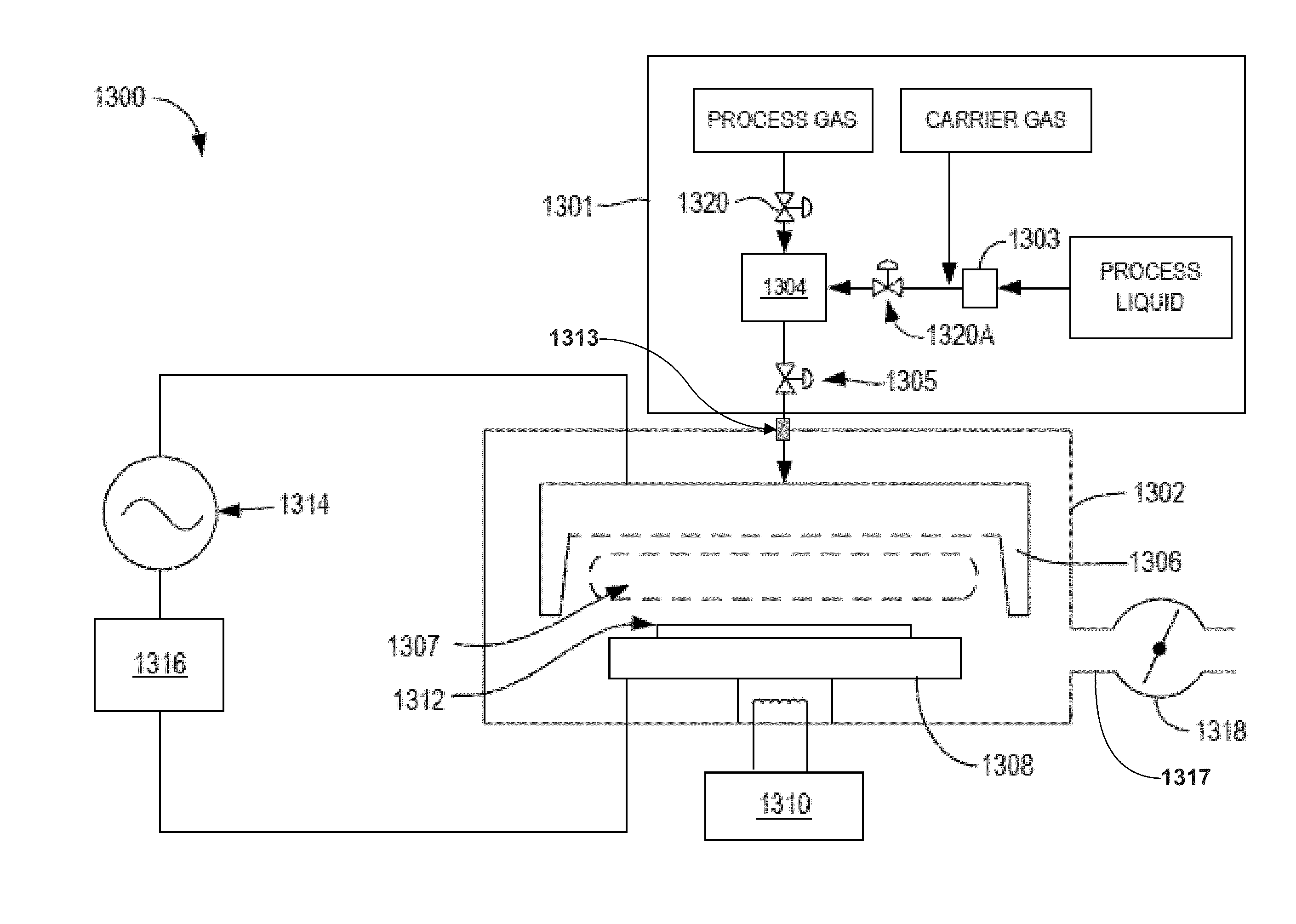
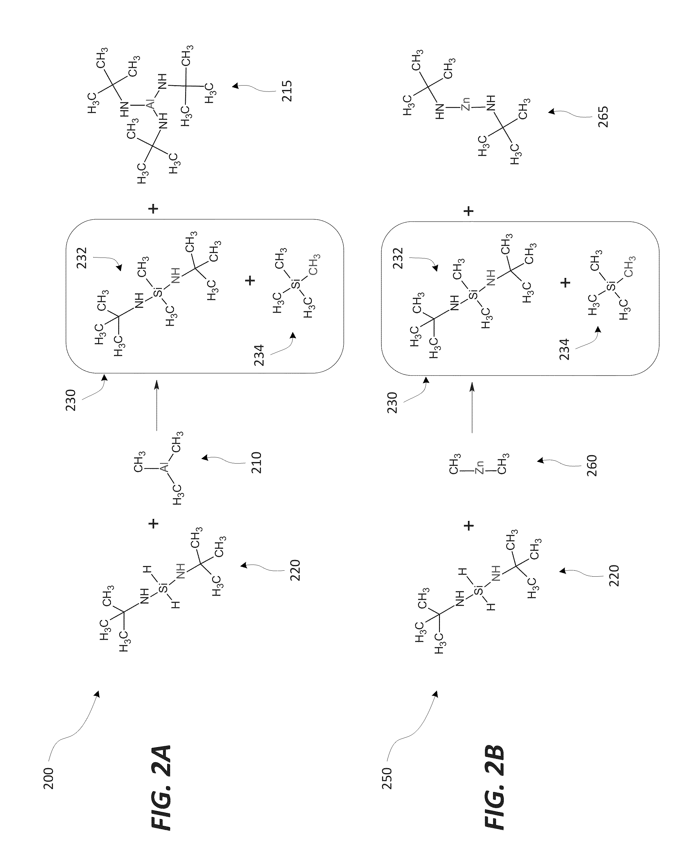
[0013]In general, a chemical reaction may be referred to as a metathesis reaction, or exchange reaction, or double replacement reaction if it is of the type:

A-B+C-D→A-D+C—B  (Eq. 1),

wherein parts of two reacting chemical species swap places. A concrete example, for instance is

AgNO3+HCl→HNO3+AgCl  (Eq. 2),

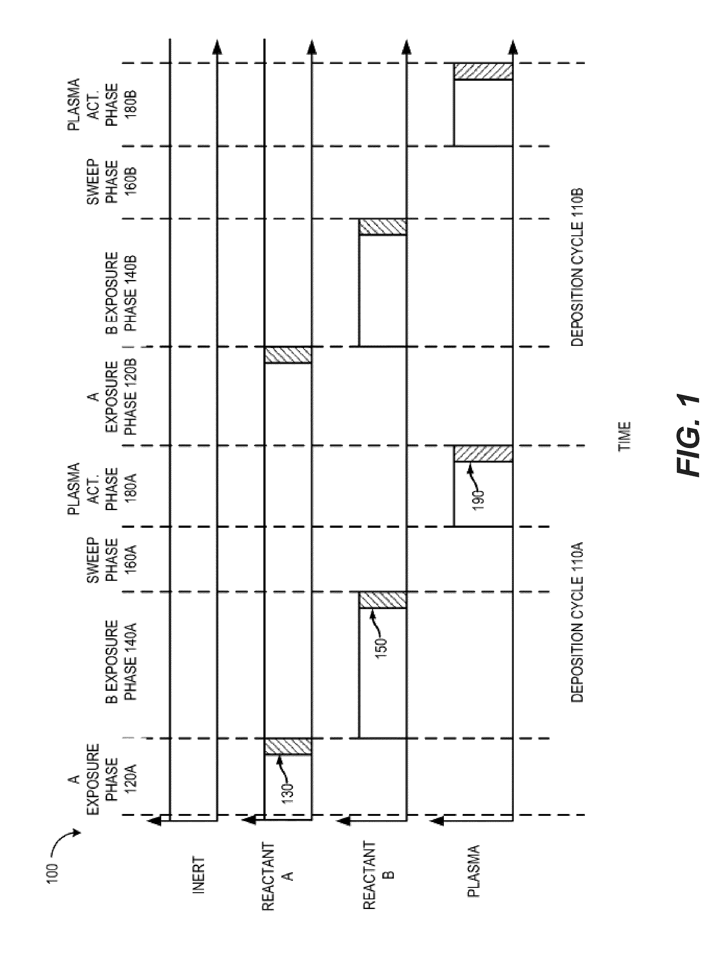
wherein after the reaction, the Cl functional group has swapped places with the NO3 functional group originally attached to the Ag atom. In some cases, these sorts of chemical reactions—involving the swapping of bonding partners—may be useful for depositing films in semiconductor device fabrication. One such application is to the deposition of SiC and / or SiCN films. In some cases, films of SiC and / or SiCN deposited via metathesis reactions are capable of meeting step-coverage, fill, defect, reliability, and electrical requirements for the nominal 1X nm memory and 16 / 12 nm generation logic nodes. In some cases, these films may be advantageously deposited at temperatures of under 400°...


PUM

PropertyMeasurementUnit
Adsorption entropyaaaaaaaaaa

Abstract

Disclosed herein are methods of forming SiC/SiCN film layers on surfaces of semiconductor substrates. The methods may include introducing a silicon-containing film-precursor and an organometallic ligand transfer reagent into a processing chamber, adsorbing the silicon-containing film-precursor, the organometallic ligand transfer reagent, or both onto a surface of a semiconductor substrate under conditions whereby either or both form an adsorption-limited layer, and reacting the silicon-containing film-precursor with the organometallic ligand transfer reagent, after either or both have formed the adsorption-limited layer. The reaction results in the forming of the film layer. In some embodiments, a byproduct is also formed which contains substantially all of the metal of the organometallic ligand transfer reagent, and the methods may further include removing the byproduct from the processing chamber. Also disclosed herein are semiconductor processing apparatuses for forming SiC/SiCN film layers.

Description

CROSS-REFERENCE TO RELATED APPLICATIONS[0001]This application is a continuation-in-part of U.S. patent application Ser. No. 13 / 084,399, titled “PLASMA ACTIVATED CONFORMAL FILM DEPOSITION,” and filed Apr. 11, 2011, which is incorporated herein by reference in its entirety and for all purposes.[0002]U.S. patent application Ser. No. 13 / 084,399 was filed claiming the benefit of U.S. provisional patent application No. 61 / 324,710, filed Apr. 15, 2010, and U.S. provisional patent application No. 61 / 372,367, filed Aug. 10, 2010, and U.S. provisional patent application No. 61 / 379,081, filed Sep. 1, 2010, and U.S. provisional patent application No. 61 / 417,807, filed Nov. 29, 2010, each of which is incorporated herein by reference in its entirety and for all purposes.BACKGROUND[0003]Various thin film layers of semiconductor devices may be deposited with atomic layer deposition (ALD) processes. However, some ALD processes produce unwanted byproducts such as ammonium chloride. Some ALD processes...

Claims


Application Information

Patent Timeline
IPC IPC(8): H01L21/02
CPCH01L21/0226H01L21/02274C23C16/36C23C16/4554C23C16/45542C23C16/45553C23C16/325H01L21/02167H01L21/0228H01L21/02208C23C16/45529H01L21/0217C23C16/45525C23C16/52H01L21/02211
Inventor LAVOIE, ADRIEN
Owner NOVELLUS SYSTEMS
Why Eureka
Try Eureka