
Eureka
For R&D, Eureka makes reading and utilizing patents & technical documents easy.
Eureka AIR
Designed for self-driven R&D workflows. Generate viable solutions, solve complex R&D challenges, empower your innovation with AI.

Eureka Materials
Designed for material experts only. Revolutionize your material R&D, from search, analyze, to developing new materials.

TechResearch
Generate reliable direction feasibility study reports for your R&D in just a few steps.

TechSeek
Discover and master advanced knowledge NOW. Basics, ideas, possibilities, all at once.

TechMind
As an expert in R&D Theories, TechMind can generates customized viable solutions instantly.

TechRisk
Analyze your overall solution with one click, know your potential R&D risks in advance.

TechMonitor
Get weekly tech updates, stay abreast of the latest tech innovations and key insights.
Integrated metal oxide chemical sensor
- Summary
- Abstract
- Description
- Claims
- Application Information
AI Technical Summary
Benefits of technology
Problems solved by technology
Method used
Image

Examples
Embodiment Construction
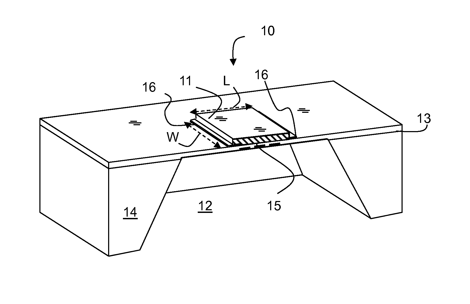
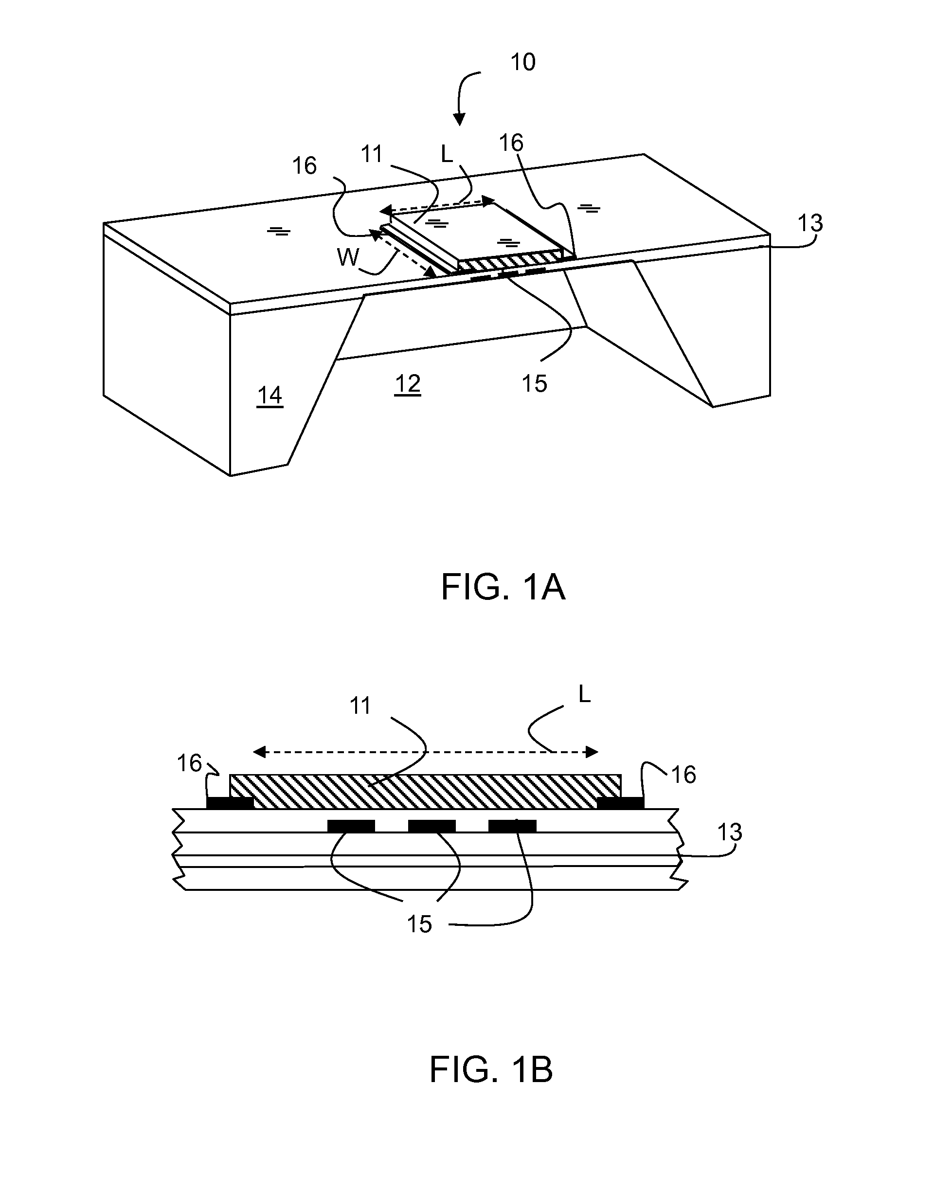
[0029]A gas sensor 10 with a sensing layer 11 of metal oxide is shown in FIGS. 1A and 1B. The sensor is integrated with a CMOS circuitry (not shown) on a single chip. Parts of the CMOS layers 13 and handle layer 14 required for the CMOS circuit are etched away to form a MEMS device with a cavity 12 at the location of the sensor. The remaining layers 13 form a thin membrane to support the actual sensor 10.
[0030]Embedded within the layers 13 are conducting elements forming a heater 15 to provide a local source of heat to heat the metal oxide 11 during operation of the sensor. The membrane structure above the cavity 12 provides an inherent thermal insulation for the rest of the substrate with the CMOS circuit. Also, the temperature can rise rapidly around the metal oxide layer 11, while the thicker part of chip reacts due to its thermal inertia with a slower rise of temperature. By controlling the heater accordingly, the metal oxide can be heated to its operating temperature of 250 to ...
PUM
 Abstract
Description
Claims
Application Information
 - R&D Engineer
- R&D Manager
- IP Professional
- Industry Leading Data Capabilities
- Powerful AI technology
- Patent DNA Extraction
Browse by: Latest US Patents, China's latest patents, Technical Efficacy Thesaurus, Application Domain, Technology Topic, Popular Technical Reports.
© 2024 PatSnap. All rights reserved.Legal|Privacy policy|Modern Slavery Act Transparency Statement|Sitemap|About US| Contact US: help@patsnap.com