Eureka AIR delivers breakthrough ideas for toughest innovation challenges, trusted by R&D personnel around the world.

Display device

Active Publication Date: 2011-08-18
JAPAN DISPLAY INC +1
View PDF4 Cites 5 Cited by
  • Summary
  • Abstract
  • Description
  • Claims
  • Application Information

AI Technical Summary

Benefits of technology

[0011]In order to prevent this, a barrier metal such as MoW is formed as an underlayer for the Al alloy in the source electrode. While the barrier metal is formed by sputtering, the barrier metal in the state as sputtered has no sufficient barrier effect for Al. Accordingly, after the barrier metal is formed, it is necessary to subject the same to a heat treatment to increase the density of the barrier metal thereby improving the barrier effect. However, the heat treatment step results in a phenomenon of oxidizing the battier metal. When the barrier metal is oxidized, Al is oxidized thereby resulting in a problem of increasing the contact resistance with respect to the Al alloy.
[0020]The present invention intends to prevent the increase of the contact resistance in the through-hole.
[0022]First, after the lower layer of the barrier metal is formed by sputtering, the substrate is taken out of a chamber and subjected to a heat treatment. The heat treatment is performed for increasing the density of the film structure in the lower layer of the barrier metal to provide the barrier effect. Subsequently, the substrate is again loaded in the vacuum chamber, the upper layer, the Al alloy, and the cap metal of the barrier metal are formed continuously by sputtering.
[0023]While the lower layer of the barrier metal is oxidized when taken out into the atmospheric air, the layer is covered by the upper layer of the barrier metal sputtered subsequently in vacuum, and the barrier metal and the Al alloy are not in contact with each other. Thus the Al in the Al alloy is not oxidized and the contact resistance can be kept lower.
[0024]According to the invention, since the contact resistance between the TFT and the drain electrode or the source electrode is decreased, rise of the driving voltage can be suppressed in the organic EL display device and, as a result, the emission efficiency of the organic EL display device can be improved.
[0025]Further, in the liquid crystal display device, since the contact resistance between the TFT and the source electrode in the through-hole can be decreased, the operation speed of the driving circuit can be increased, particularly, when the driving circuit is formed by the TFT.

Problems solved by technology

While the barrier metal is formed by sputtering, the barrier metal in the state as sputtered has no sufficient barrier effect for Al.
However, the heat treatment step results in a phenomenon of oxidizing the battier metal.
When the barrier metal is oxidized, Al is oxidized thereby resulting in a problem of increasing the contact resistance with respect to the Al alloy.

Method used


Image

  • Display device
  • Display device
  • Display device

Examples


example 1

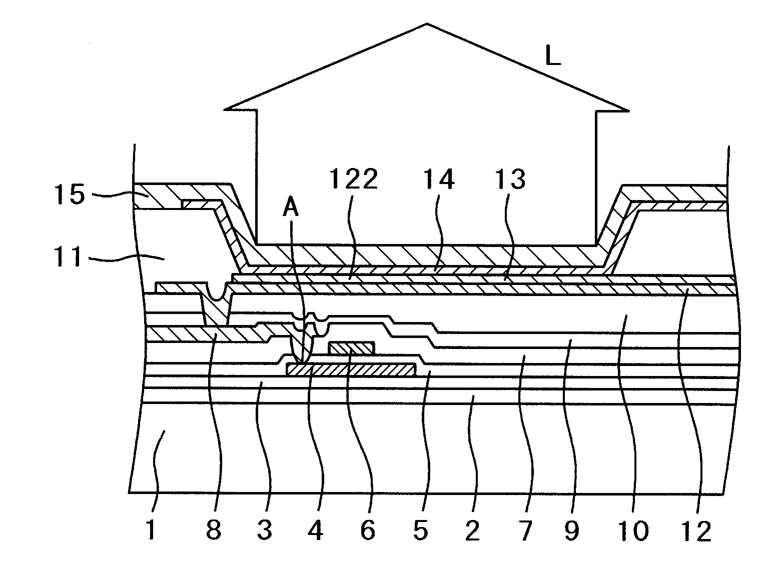
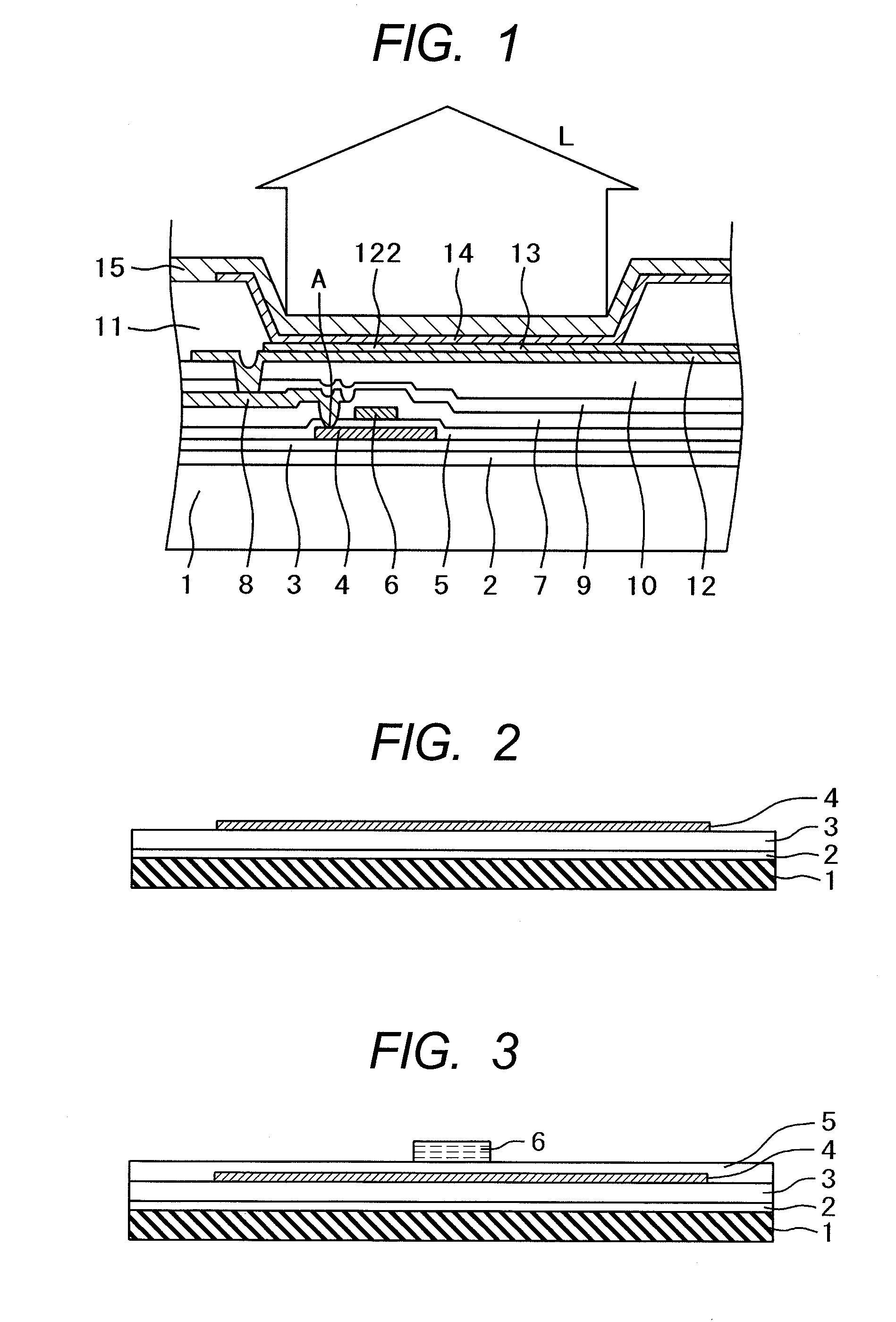
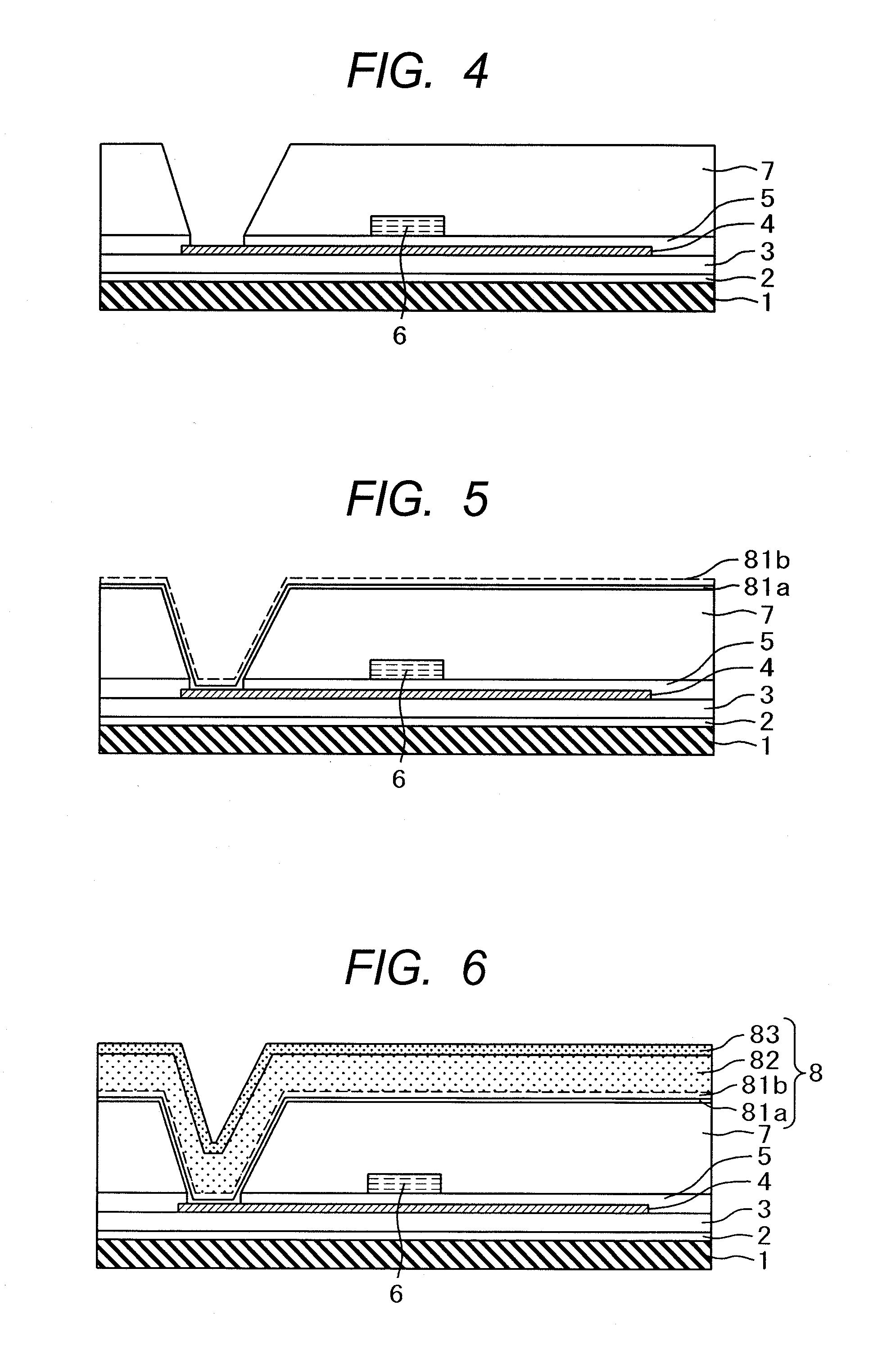
[0056]FIGS. 2 to 6 show a process up to the formation of the source electrode 8 in the organic EL display device shown in FIG. 1. Since FIGS. 2 to 4 are identical with FIGS. 8 to 10 that have been explained for the existent example, explanation for them is to be omitted. That is, the process up to the state in FIG. 4 where the through-hole is formed in the interlayer insulation film 7 and the gate insulation film 5 is identical with that in the existent example.

[0057]Similarly to the existent example, the source electrode 8 has the three layered structure comprising the barrier metal, the Al alloy 82, and the cap metal 83. The feature of the invention is to deposit the barrier metal film divided into two layers. That is, a lower layer 81a of the battier metal serves to prevent the Al atoms from diffusing into the poly-Si semiconductor layer 4. This is a primary role as the barrier metal. An upper layer 81b of the barrier metal serves to decrease the contact resistance in the through...


PUM


Abstract

A contact resistance in a through-hole with a source or a drain electrode connected to a TFT is decreased, thereby improving the operation efficiency of a display device.In the through-hole, a source portion of the TFT is connected to a source electrode 8. The source electrode 8 is formed of three layers comprising a barrier metal, an Al alloy 82, and a cap metal 83. The barrier metal is divided into a lower layer 81a in contact with the semiconductor layer and an upper layer 81b in contact with the Al alloy. The lower layer 81a of the barrier metal is formed by sputtering, the lower layer 81a is heat-treated and, subsequently, an upper layer 81b of the base metal, the Al alloy 82, and the cap metal 83 are formed continuously by sputtering. Since the upper layer 81b of the barrier metal in contact with the Al alloy 82 is not oxidized, increase in the contact resistance in the through-hole can be prevented.

Description

CLAIM OF PRIORITY[0001]The present application claims priority from Japanese Patent Application JP 2010-032439 filed on Feb. 17, 2010, the content of which is hereby incorporated by reference into this application.BACKGROUND OF THE INVENTION[0002]1. Field of the Invention[0003]The present invention relates to a display device. The invention more particularly relates to an active matrix type display device which is improved in the response speed or the emission efficiency by decreasing the contact resistance in a through-hole.[0004]2. Description of the Related Art[0005]In an organic EL display device or a liquid crystal display device, scanning lines are extended in a first direction and arranged in a second direction. Further, video signal lines are extended in the second direction and arranged in the first direction. Areas surrounded by the scanning lines and the video lines define pixels and a thin film transistor (TFT) is formed for each of the pixels.[0006]The organic EL displa...

Claims


Application Information

Patent Timeline
IPC IPC(8): G02F1/136H01L33/08H01J1/62
CPCH01L27/124H01L27/3248H01L29/41733G02F1/136227H01L29/78675H01L27/1222H01L27/3276H01L29/78666G02F1/13306H10K59/123H10K59/131
Inventor ASAI, TAROGOTOH, JUNOUE, EIJIASUMA, HIROAKINAKAYASHIKI, KATSUMIKURITA, MAKOTO
Owner JAPAN DISPLAY INC
Why Eureka
Eureka Blog
Learn More