Manufacturing method of thin film transistor

Inactive Publication Date: 2012-09-13
CHUNGHWA PICTURE TUBES LTD
View PDF9 Cites 8 Cited by
  • Summary
  • Abstract
  • Description
  • Claims
  • Application Information

AI Technical Summary

Benefits of technology

[0010]In the present invention, the localized laser treatment is employed to selectively lower the electrical resistivity of the oxide semiconductor layer within specific regions. The purpose of lowering the contact resistance between the oxide semiconductor layer and the source/drain electrodes and enhancin

Problems solved by technology

However, the amorphous silicon thin film transistor may not be good enough to satisfy requirements of foreseeable high performance display devices, because the electrical mobility of the amorphous silicon thin film transistor, which is mainly determined by material properties of amorphous silicon, can not be effectively improved by process tuning or design modification.
However, because of process issues such as high process complexity and worse uniformity, which is ma

Method used


Image

  • Manufacturing method of thin film transistor
  • Manufacturing method of thin film transistor
  • Manufacturing method of thin film transistor

Examples


Embodiment Construction

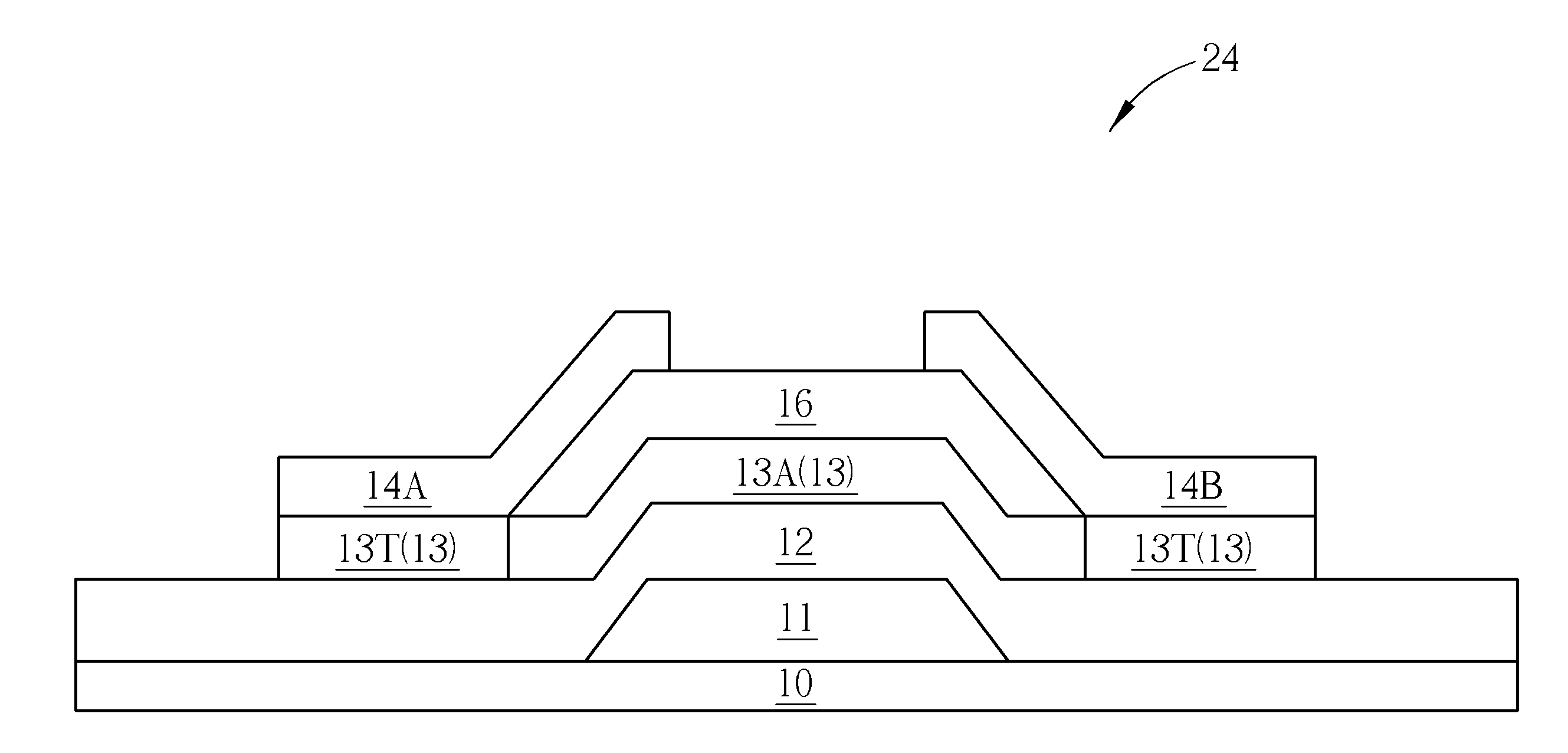
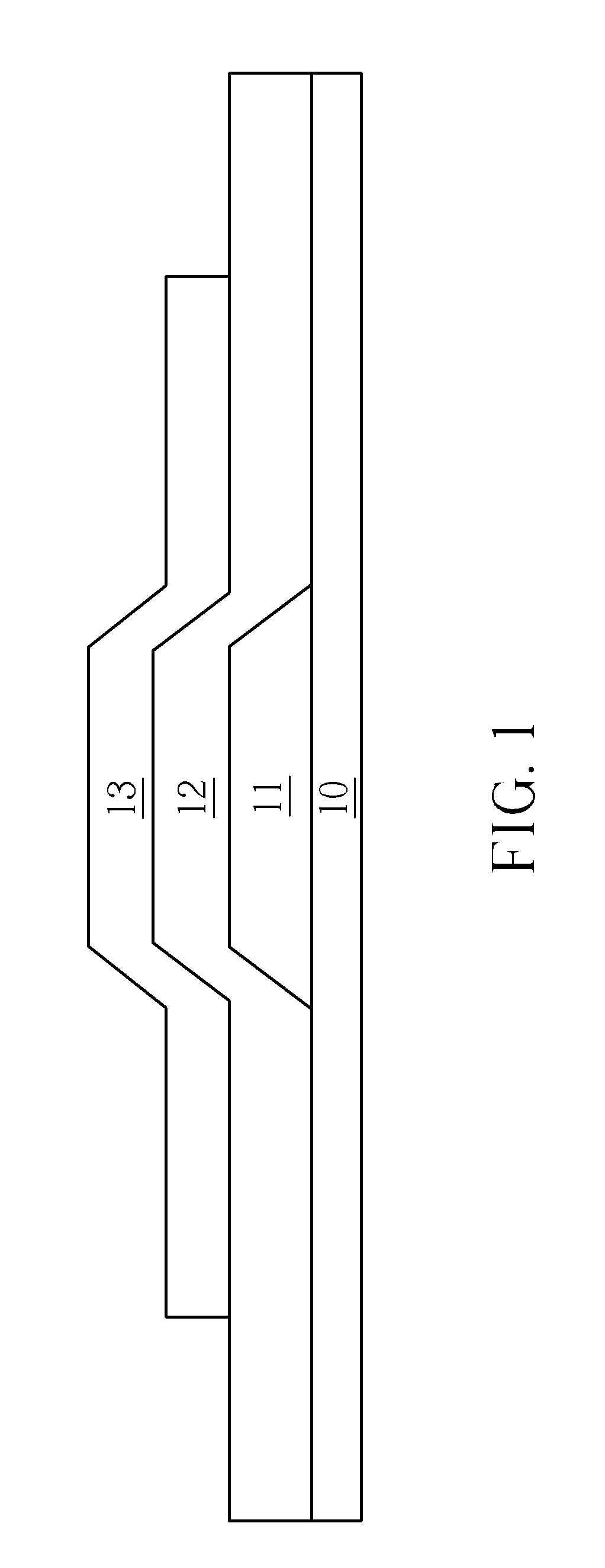
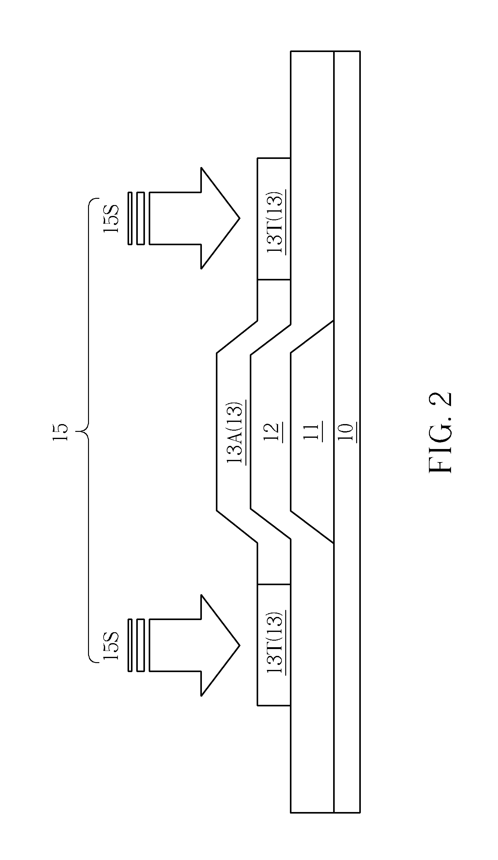
[0017]Certain terms are used throughout the description and following claims to refer to particular components. As one skilled in the art will understand, electronic equipment manufacturers may refer to a component by different names. This document does not intend to distinguish between components that differ in name but not function. In the following description and in the claims, the terms “include” and “include” are used in an open-ended fashion, and thus should be interpreted to mean “include, but not limited to . . . ” In addition, to simplify the descriptions and make it more convenient to compare between each embodiment, identical components are marked with the same reference numerals in each of the following embodiments. Please note that the figures are only for illustration and the figures may not be to scale.

[0018]Please refer to FIGS. 1-3. FIGS. 1-3 are schematic diagrams illustrating a manufacturing method of a thin film transistor according to the first preferred embodi...


PUM


Abstract

A manufacturing method of thin film transistors is provided. The manufacturing method includes: providing a substrate; forming a gate electrode; forming a gate insulating layer; forming a patterned oxide semiconductor layer; forming a source electrode and a drain electrode; and executing a localized laser treatment. A laser beam is used to irradiate at least a part of the patterned oxide semiconductor layer in the localized laser treatment. An electrical resistitivity of the patterned oxide semiconductor layer irradiated by the laser beam is lower than an electrical resistitivity of the patterned oxide semiconductor layer without being irradiated by the laser beam.

Description

BACKGROUND OF THE INVENTION[0001]1. Field of the Invention[0002]The present invention relates to a manufacturing method of a thin film transistor, and more particularly, to a manufacturing method of a thin film transistor with an oxide semiconductor layer, wherein a localized laser treatment is employed to lower a contact resistance between the oxide semiconductor layer and the source / drain electrode.[0003]2. Description of the Prior Art[0004]In recent years, applications of flat display devices are rapidly developed. Electronics, such as televisions, cell phones, mobiles, and refrigerators, are installed with flat display devices. A thin film transistor (TFT) is a kind of semiconductor devices commonly used in the flat display device, such as a liquid crystal display (LCD), an organic light emitting diode (OLED) display, and an electronic paper (E-paper). The thin film transistor is employed to control voltage and / or current of a pixel of the flat display device for presenting a br...

Claims


Application Information

Patent Timeline
IPC IPC(8): H01L21/336
CPCH01L29/7869
Inventor CHIANG, SHIN-CHUANLAI, YU-HAOLI, HUAI-AN
Owner CHUNGHWA PICTURE TUBES LTD
Why Eureka
Try Eureka