Method for fabricating copper-based interconnections for semiconductor device

Inactive Publication Date: 2006-01-26
KOBE STEEL LTD
View PDF9 Cites 23 Cited by
  • Summary
  • Abstract
  • Description
  • Claims
  • Application Information

AI Technical Summary

Benefits of technology

[0017] The present invention easily yields embedded Cu-based interconnections by embedding a Cu-based metal into grooves such as interconnection contact holes and contact trenches without clearance in the production of semiconductor devices such as silic

Problems solved by technology

Such a device, however, has an increased interconnection resistance with a decreasing size and an increasing packing density of its interconnection circuit, and the increased interconnection resistance causes delay of signal transmission.
The resulting interconnection grooves and interlayer contact holes have decreasing widths and diameters, respectively, and have increasing aspect ratios (the ratio of the depth to the diameter) The process for fabricating Cu interconnections by electrochemical deposition, however, cannot satisfactorily embed the Cu interconnection material into grooves having minute dimensions.
Thus, Cu cannot significantly perfectly embedded into via holes having high aspect ratios, and via holes and trenches having small diameters with interconnection width of 100 nm or less.
Particularly, on the interconnection design rule of 0.1 μm or less, the via holes and trenches have further decreasing dimensions and further increasing aspect ratios, and the Cu-based material cannot significantly be embedded thereinto completely, which fails to provide reliable interconnections.
The conventional da

Method used


Image

  • Method for fabricating copper-based interconnections for semiconductor device
  • Method for fabricating copper-based interconnections for semiconductor device
  • Method for fabricating copper-based interconnections for semiconductor device

Examples


example 1

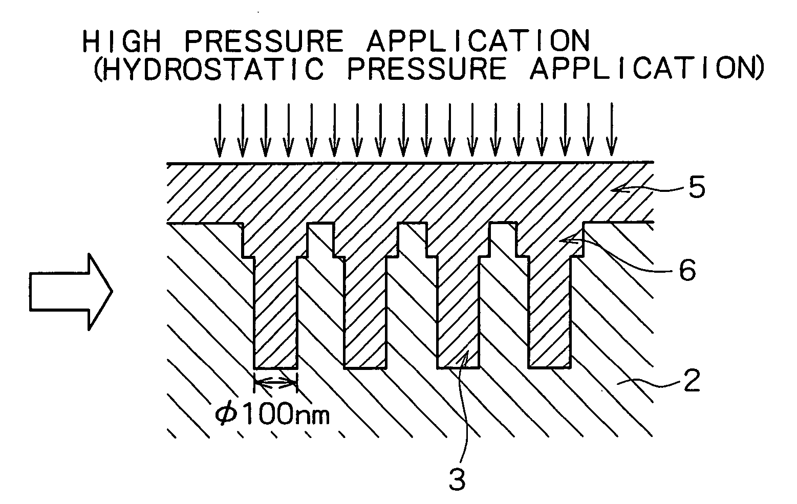
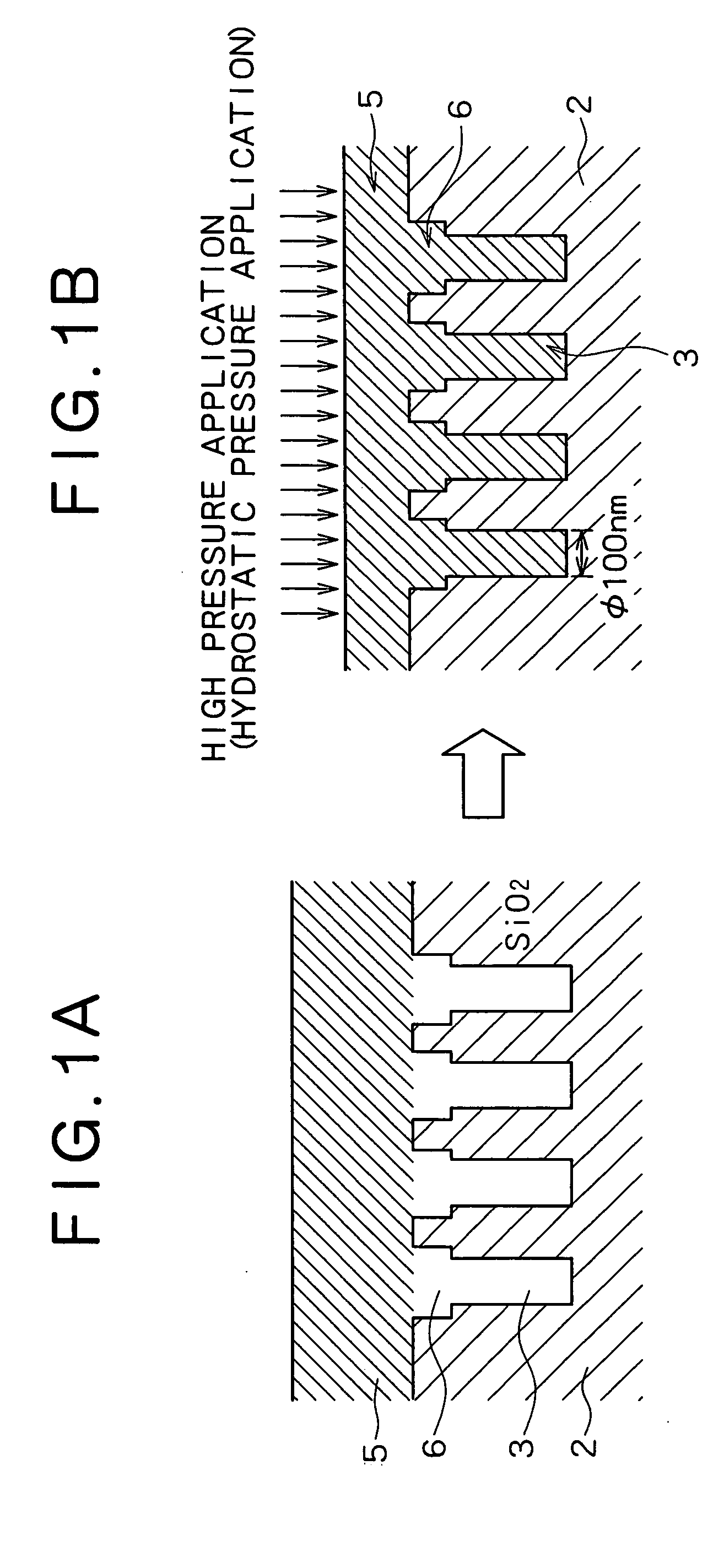
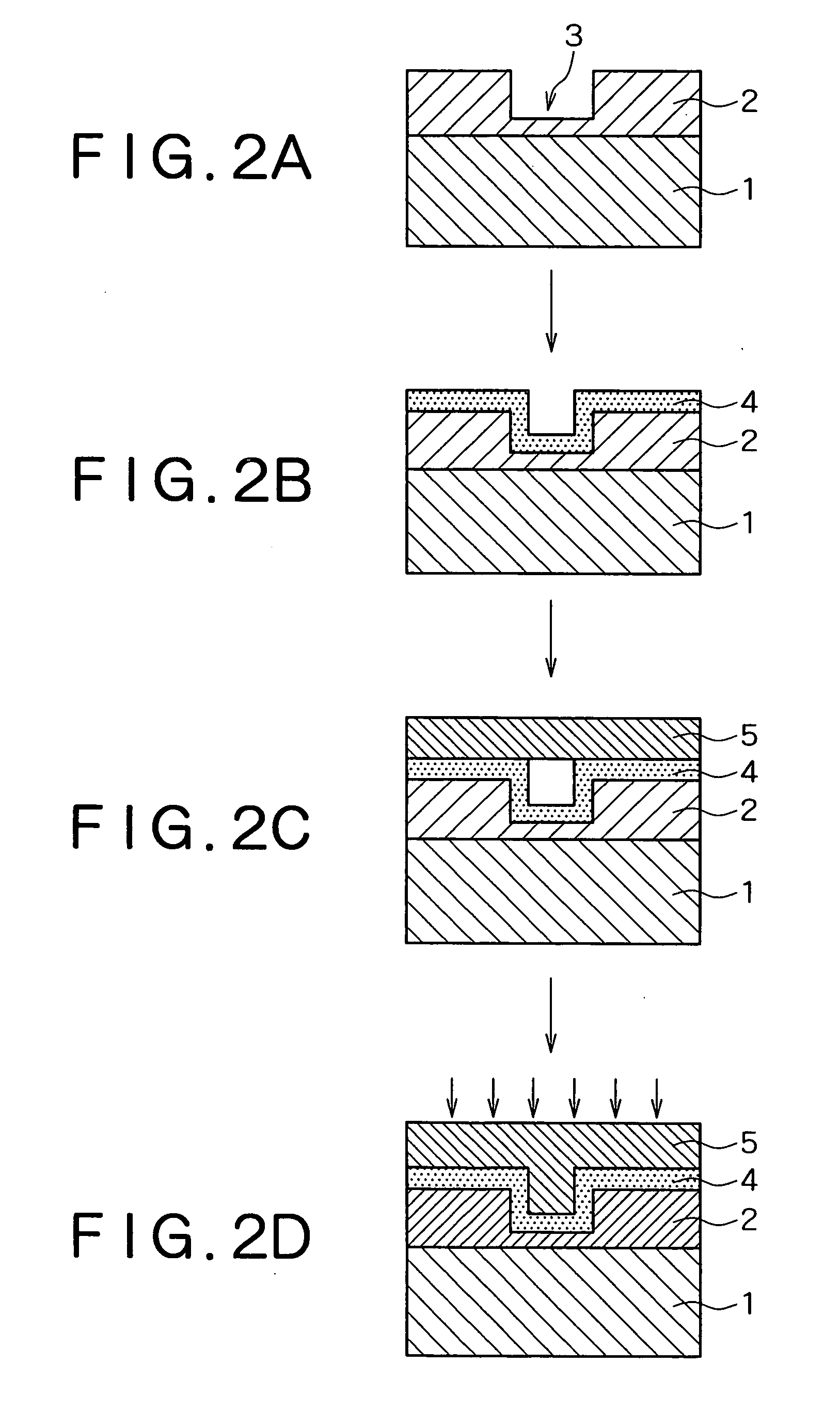
[0064] Interconnects were formed in a semiconductor device sequentially in accordance with the processes shown in the schematic sectional views of FIGS. 2A, 2B, 2C and 2D. Specifically, a large number of via hole 3 having a diameter of 0.18 μm and a pitch of 450 nm was formed on a dielectric film (TEOS film: SiOF film) 2 which had been deposited on an 8-inch silicon wafer 1 to thereby yield a test element group (TEG) (FIG. 2A). In this connection, only one via hole 3 is illustrated in FIG. 2A. A thin film of TaN was deposited on a surface of TEG by reactive sputtering in an atmosphere of Ar and N2 gas to thereby deposit a barrier layer (TaN thin film) 4 having a thickness of 50 nm on the bottom and side of the via hole 3 (FIG. 2B).

[0065] Next, a pure Cu thin film 5 having a thickness of 7500 angstroms was deposited on the TEG by sputtering in an atmosphere of Ar gas or in an atmosphere of a gaseous mixture of Ar and H2 so that an opening of the via hole 3 was fully bridged by the C...

example 2

[0074] A barrier layer (TaN thin film) 4 having a thickness of 50 nm was deposited on the bottom and side of a via hole 3 of a TEG by the procedure of Example 1, and a pure Cu thin film 5 having a thickness of 7500 angstroms was deposited thereon by sputtering so that the Cu thin film 5 fully bridged the opening of the via hole 3. The Cu thin film 5 was deposited at the following constant sputtering gas pressure and discharge power density using the following sputtering gas while varying the substrate temperature in a range from −25° C. to 200° C. [0075] Sputtering gas pressure: 2×10⁻³ Torr [0076] Sputtering gas: Ar−20% H2 [0077] Discharge power density: 3.5 W / cm2

[0078] Next, the TEG was subjected to high temperature and high pressure treatment by the procedure of Example 1, and how Cu was embedded in the via hole 3 was determined. The results are shown in FIG. 4. FIG. 4 is a graph showing the relationship between the filling percentage of Cu and the substrate temperature in deposi...

example 3

[0079] A barrier layer (TaN thin film) 4 having a thickness of 50 nm was deposited on the bottom and side of a via hole 3 of a TEG by the procedure of Example 1, and a pure Cu thin film 5 having a thickness of 7500 angstroms or a Cu alloy thin film 5 having a thickness of 7500 angstroms was deposited thereon by sputtering so that the thin film 5 fully bridged the opening of the via hole 3. In this procedure, the pure Cu thin film 5 was deposited with a pure Cu target, and the Cu alloy thin film 5 was deposited with a Cu alloy target containing 2.0 atomic percent of Dy. The sputtering gas pressure, type of sputtering gas, discharge power density and substrate temperature are as shown in Table 1 (Deposition Condition 1 or Deposition Condition 2).

TABLE 1Deposition parameterCondition 1Condition 2Sputtering gas pressure (Torr)2 × 10−32 × 10−3Type of sputtering gaspure ArAr-20% H2Discharge power density (W / cm2)3.53.5Substrate temperature (° C.)room temperature−20

[0080] The TEG was then ...


PUM


Abstract

Cu-based interconnections are fabricated in a semiconductor device by depositing a thin film of Cu or Cu alloy on a dielectric film by sputtering, the dielectric film having trenches and/or via holes at least one groove and being arranged on or above a substrate, and carrying out high temperature and high pressure treatment to thereby embed the Cu or Cu alloy into the trenches and/or via holes, in which the sputtering is carried out at a substrate temperature of −20° C. to 0° C. using, as a sputtering gas, a gaseous mixture containing hydrogen gas and an inert gas in a ratio in percentage of 5:95 to 20:80.

Description

BACKGROUND OF THE INVENTION [0001] 1. Field of the Invention [0002] The present invention relates to a method for fabricating interconnections of pure Cu or a Cu alloy (hereinafter generically referred to as “Cu-based metal”) in semiconductor devices. Specifically, it relates to a method for fabricating Cu-based interconnections in semiconductor devices, such as Si semiconductor devices, typified by ultra-large scale integrated circuits (ULSL) by fabricating a thin film of a Cu-based metal on a groove, such as a via hole or a trench, arranged in a dielectric film by sputtering (physical vapor deposition), and embedding the Cu-based metal into the groove by reflowing at high temperature and high pressure to thereby fabricate the Cu-based interconnection. [0003] 2. Description of the Related Art [0004] The design rule of semiconductor devices such as large-scale integrated circuits (LSIs) has more and more reduced shrank for larger packing densities and higher-speed signal transmissio...

Claims


Application Information

Patent Timeline
IPC IPC(8): H01L21/4763H01L21/44
CPCH01L21/76882H01L21/2855H01L21/28
Inventor ONISHI, TAKASHIYASUNAGA, TATSUYAFUJII, HIDEOYOSHIKAWA, TETSUYAMUNEMASA, JUN
Owner KOBE STEEL LTD
Why Eureka
Try Eureka