Eureka AIR delivers breakthrough ideas for toughest innovation challenges, trusted by R&D personnel around the world.

Semiconductor structure and manufacturing method thereof

Active Publication Date: 2017-04-06
UNITED MICROELECTRONICS CORP
View PDF6 Cites 3 Cited by
  • Summary
  • Abstract
  • Description
  • Claims
  • Application Information

AI Technical Summary

Benefits of technology

The present invention is about a semiconductor structure and a method to improve its performance. The invention includes an oxide-containing layer and / or a metal oxide-containing layer between the epitaxial region and the contact structure. This helps to lower the Schottky barrier height between the layers, which in turn reduces the contact resistance and improves device performance.

Problems solved by technology

The development of semiconductor integrated circuit technology progresses continuously and circuit designs in products of the new generation become smaller and more complicated than those of the former generation.

Method used


Image

  • Semiconductor structure and manufacturing method thereof
  • Semiconductor structure and manufacturing method thereof
  • Semiconductor structure and manufacturing method thereof

Examples


Embodiment Construction

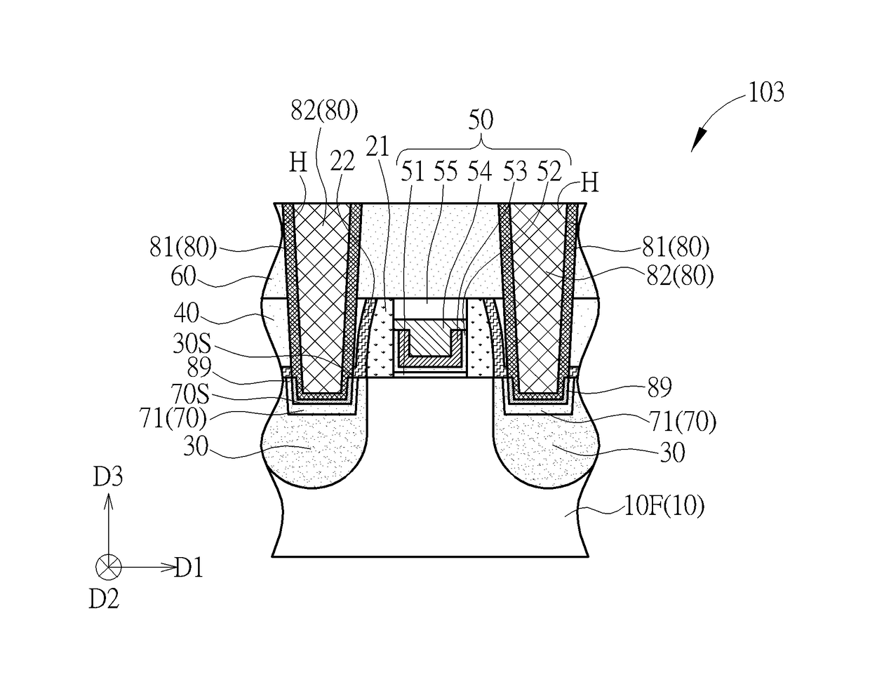
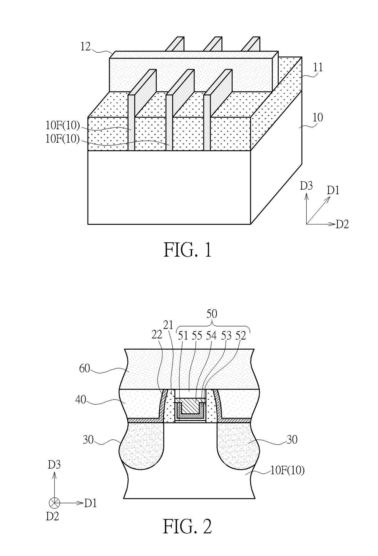
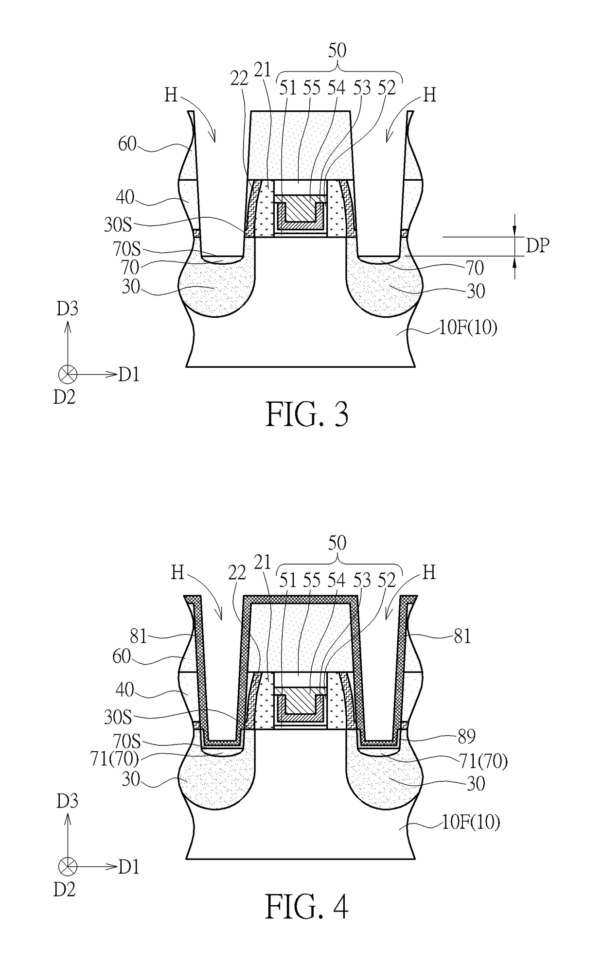
[0018]Please refer to FIGS. 1-6. FIGS. 1-5 are schematic drawings illustrating a manufacturing method of a semiconductor structure according to a first embodiment of the present invention, and FIG. 6 is an enlarged schematic drawing illustrating an epitaxial region in FIG. 5. The manufacturing method of the semiconductor structure in this embodiment includes the following steps. As shown in FIG. 1, a semiconductor substrate 10 is provided. The semiconductor substrate 10 in this embodiment may include a silicon substrate, an epitaxial silicon substrate, a silicon germanium substrate, a silicon carbide substrate, or a silicon-on-insulator (SOI) substrate, but not limited thereto. The semiconductor substrate 10 may also have a plurality fin structures 10F extending in a first direction D1 according to design requirements, and the fin structures 10F may be separated from one another by shallow trench isolation (STI) 11, but not limited thereto. Additionally, a dummy gate 12 may be forme...


PUM


Abstract

A manufacturing method of a semiconductor structure includes the following steps. An epitaxial region is formed in a semiconductor substrate. A dielectric layer is formed on the epitaxial region, and a contact hole is formed in the dielectric layer. The contact hole exposes a part of the epitaxial region, and an oxide-containing layer is formed on the epitaxial region exposed by the contact hole. A contact structure is formed in the contact hole and on the oxide-containing layer. The oxide-containing layer is located between the contact structure and the epitaxial region. A semiconductor structure includes the semiconductor substrate, at least one epitaxial region, the contact structure, the oxide-containing layer, and a silicide layer. The contact structure is disposed on the epitaxial region. The oxide-containing layer is disposed between the epitaxial region and the contact structure. The silicide layer is disposed between the oxide-containing layer and the contact structure.

Description

BACKGROUND OF THE INVENTION[0001]1. Field of the Invention[0002]The present invention relates to a semiconductor structure and a manufacturing method thereof, and more particularly, to a semiconductor structure including an oxide-containing layer formed between a contact structure and an epitaxial region for lowering the contact resistance and a manufacturing method thereof.[0003]2. Description of the Prior Art[0004]The development of semiconductor integrated circuit technology progresses continuously and circuit designs in products of the new generation become smaller and more complicated than those of the former generation. The amount and the density of the functional devices in each chip region are increased constantly according to the requirements of innovated products, and the size of each device has to become smaller accordingly. As the size of the device becomes smaller, the influence of the contact resistance at the interface between the source / drain contact and the source / d...

Claims


Application Information

Patent Timeline
IPC IPC(8): H01L29/78H01L21/02H01L21/31H01L27/088H01L21/285H01L29/26H01L29/417H01L29/45H01L29/66H01L21/311
CPCH01L29/7839H01L29/66969H01L21/02521H01L21/31H01L21/31116H01L27/088H01L29/26H01L21/28518H01L29/41725H01L29/45H01L21/28568H01L29/41766H01L29/66545H01L29/66636H01L29/66643H01L29/165H01L21/285H01L23/485H01L21/76805H01L21/76831H01L21/76843H01L21/76855H01L29/41791
Inventor HUNG, CHING-WENWU, YI-KUANWU, JIA-RONGLEE, YI-HUILIU, YING-CHENGHUANG, CHIH-SENCHEN, YI-WEI
Owner UNITED MICROELECTRONICS CORP
Why Eureka
Eureka Blog
Learn More