Eureka AIR delivers breakthrough ideas for toughest innovation challenges, trusted by R&D personnel around the world.

Chip-to-chip signal transmission system and chip-to-chip capacitive coupling transmission circuit

a capacitive coupling and transmission circuit technology, applied in the direction of electronic circuit testing, measurement devices, instruments, etc., can solve the problems of high production cost, more details of front-end and back-end ic fabrication processes revealed, and achieve the effect of improving the communication quality of capacitive coupling connections

Active Publication Date: 2014-07-31
I-SHOU UNIVERSITY
View PDF4 Cites 4 Cited by
  • Summary
  • Abstract
  • Description
  • Claims
  • Application Information

AI Technical Summary

Benefits of technology

The patent describes a system and circuit that improve communication between chips in a three-dimensional integrated circuit by using capacitive coupling. This improves the quality of the connection and allows for chip self-testing. The circuit design also addresses issues with traditional technology such as high costs and low yield rates. The technical effects include improved communication quality and chip self-testing.

Problems solved by technology

However, TSV 3D IC faces technical problems related to wafer thinning, chip stack, and heat dissipation processing.
In addition, as TSV 3D IC technology continues to advance and be applied to actual fabrication, more problems about details of the front-end and back-end IC fabrication processes are revealed.
The major disadvantages thereof are high production costs and low yield rate.
For example, the silicon substrates may be affected by the mechanical force of drilling, which lowers the yield rate of the chips.
On the other hand, for capacitive coupling interconnection technology, a testing method thereof cannot be achieved in the conventional 3D IC technology yet.

Method used


Image

  • Chip-to-chip signal transmission system and chip-to-chip capacitive coupling transmission circuit
  • Chip-to-chip signal transmission system and chip-to-chip capacitive coupling transmission circuit
  • Chip-to-chip signal transmission system and chip-to-chip capacitive coupling transmission circuit

Examples


Embodiment Construction

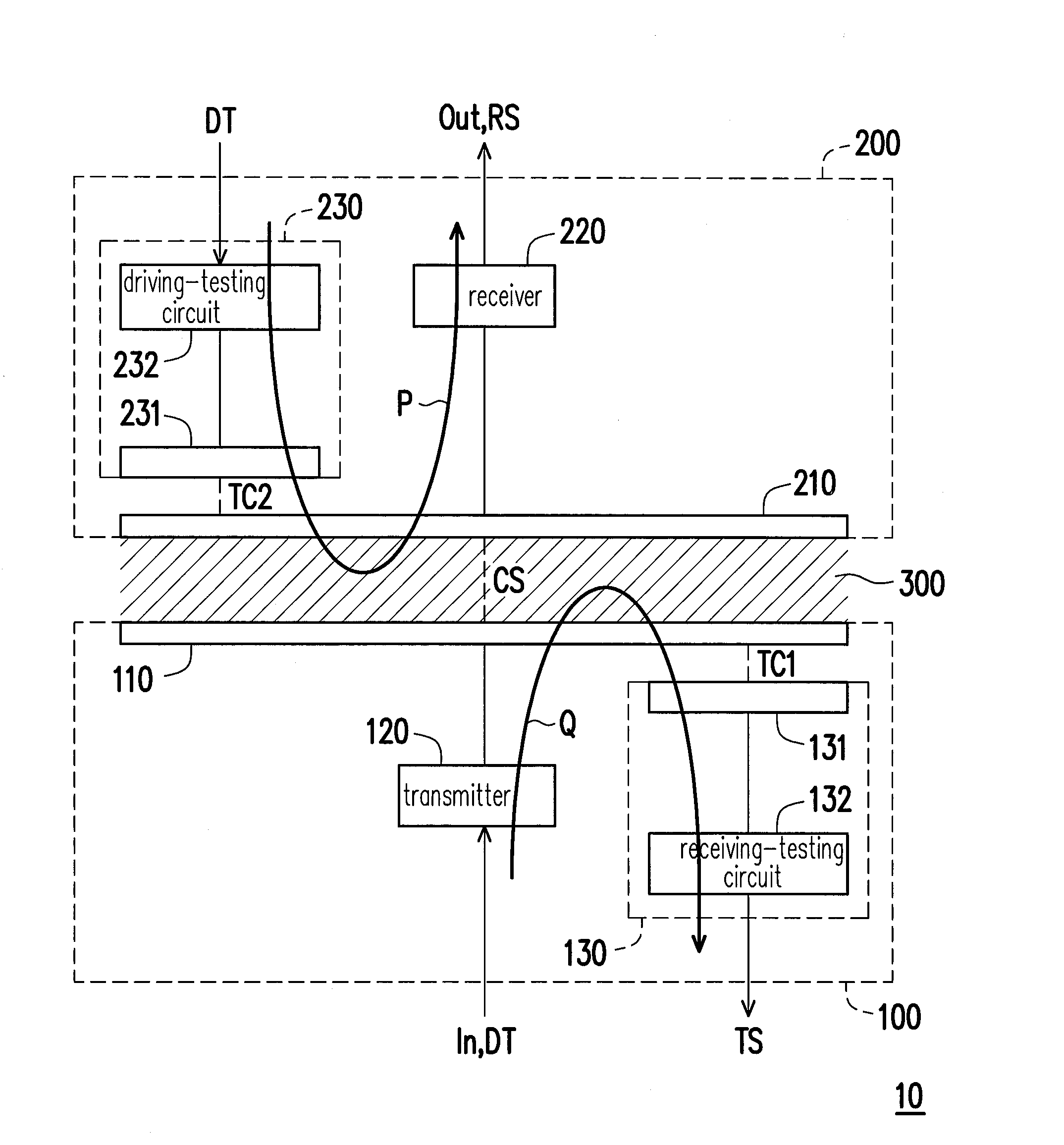
[0022]A chip-to-chip signal transmission system is disclosed hereinafter. FIG. 1 is a schematic structural diagram illustrating the chip-to-chip signal transmission system according to an embodiment of the invention. Referring to FIG. 1, a chip-to-chip signal transmission system 10 includes a chip 100 and a chip 200, and a dielectric layer 300 is disposed between the chip 100 and the chip 200. The chip 100 includes a transmission-metal-pad unit 110, a transmitter 120, and a testing unit 130. Specifically, the transmission-metal-pad unit 110 is disposed on a surface of the chip 100. The transmitter 120 is coupled to the transmission-metal-pad unit 110 for receiving input data In and outputting a chip-to-chip coupling signal CS through the transmission-metal-pad unit 110. The testing unit 130 includes a transmission-testing-metal-pad unit 131 and a receiving-testing circuit 132, and the transmission-testing-metal-pad unit 131 is coupled to the transmission-metal-pad unit 110.

[0023]The...


PUM


Abstract

A chip-to-chip signal transmission system is provided, which includes a first chip, a second chip, and a dielectric layer. A signal transmission is performed between a transmitter of the first chip and a receiver of the second chip through a transmission-metal-pad unit and a receiving-metal-pad unit. The transmitter transmits a transmission-testing-coupling signal through the transmission-metal-pad unit according to a driving-testing signal when the transmitter receives the driving-testing signal. A first testing unit receives the transmission-testing-coupling signal and outputs a transmission-testing signal according to the transmission-testing-coupling signal. A second testing unit transmits a receiving-testing-coupling signal through the receiving-metal-pad unit according to the driving-testing signal when the second testing unit receives the driving-testing signal. The receiver receives the receiving-testing-coupling signal and outputs a receiving-testing signal according to the receiving-testing-coupling signal.

Description

CROSS-REFERENCE TO RELATED APPLICATION[0001]This application claims the priority benefit of Taiwan application serial no. 102102997, filed on Jan. 25, 2013. The entirety of the above-mentioned patent application is hereby incorporated by reference herein and made a part of this specification.BACKGROUND OF THE INVENTION[0002]1. Field of the Invention[0003]The invention relates to a capacitive coupling chip-to-chip signal transmission system and particularly relates to a capacitive coupling chip-to-chip signal transmission system and a chip-to-chip capacitive coupling transmission circuit capable of self testing.[0004]2. Description of Related Art[0005]With the development of miniaturization and decreasing production costs of electronic products, IC chip miniaturization and three-dimensional stack packaging have become an important trend in the development of semiconductor technology. 3D die stacking is an emerging technology that reduces the wire length both within and across dies in...

Claims


Application Information

Patent Timeline
Patent Type & Authority Applications(United States)
IPC IPC(8): G01R31/02
CPCG01R31/02H04B17/14G01R31/312H04B5/22
Inventor HUANG, YU-JUNGCHEN, MING-KUNLIU, KAI-JEN
Owner I-SHOU UNIVERSITY
Why Eureka
Eureka Blog
Learn More