
Structure and method for manufacturing the same

a technology of structure and manufacturing method, applied in the field of structure, can solve the problems of disturbance of arrangement, disturbance of arrangement of metal structure obtained by filling metal, etc., and achieve the effect of reducing disturbances of arrangement and reducing charges

Inactive Publication Date: 2014-07-31
CANON KK
View PDF4 Cites 4 Cited by
  • Summary
  • Abstract
  • Description
  • Claims
  • Application Information

AI Technical Summary

Benefits of technology

The patent text describes a way to make a silicon mold that reduces disturbances in arrangement caused by charges. By using this mold, a method is also provided to make structures with high-aspect ratios and reduced disturbances in arrangement.

Problems solved by technology

However, in production of a mold having a high aspect ratio, it is known that in a drying step after a wet treatment, e.g., Wet cleaning or development, arrangement may be disturbed by mutual sticking of convex portions (or portions sandwiched between a recessed portion) of the mold due to the surface tension of the droplet.
If the arrangement of the mold is disturbed, the arrangement of a metal structure obtained by filling the metal is disturbed.

Method used


Image

  • Structure and method for manufacturing the same
  • Structure and method for manufacturing the same
  • Structure and method for manufacturing the same

Examples


first embodiment

[0039]In a first embodiment, a method for manufacturing a two-dimensional structure will be described. The two-dimensional structure produced according to the present embodiment can be used as a two-dimensional shield grating in an X-ray Talbot interference method.

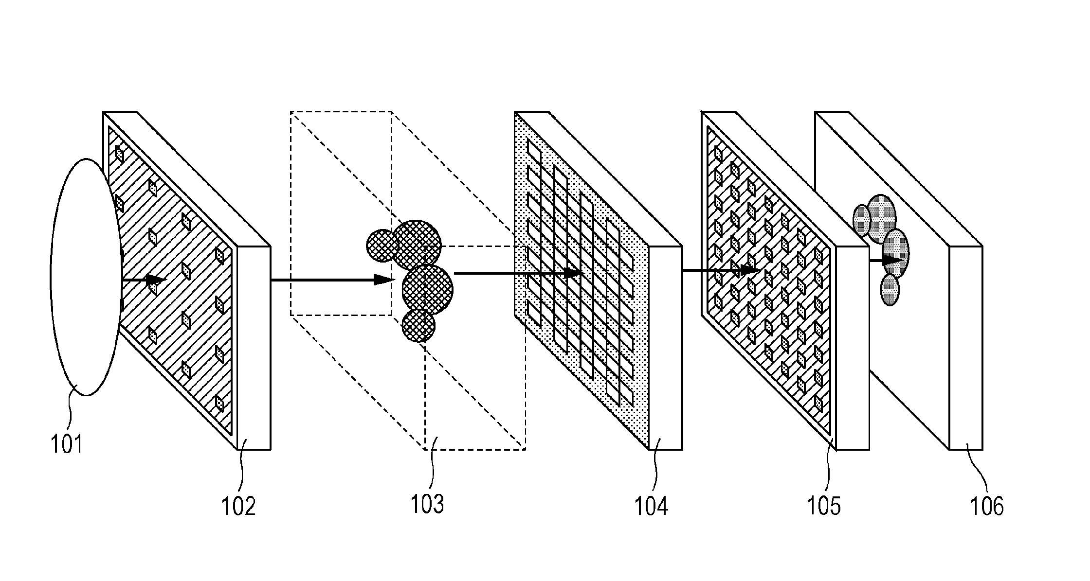
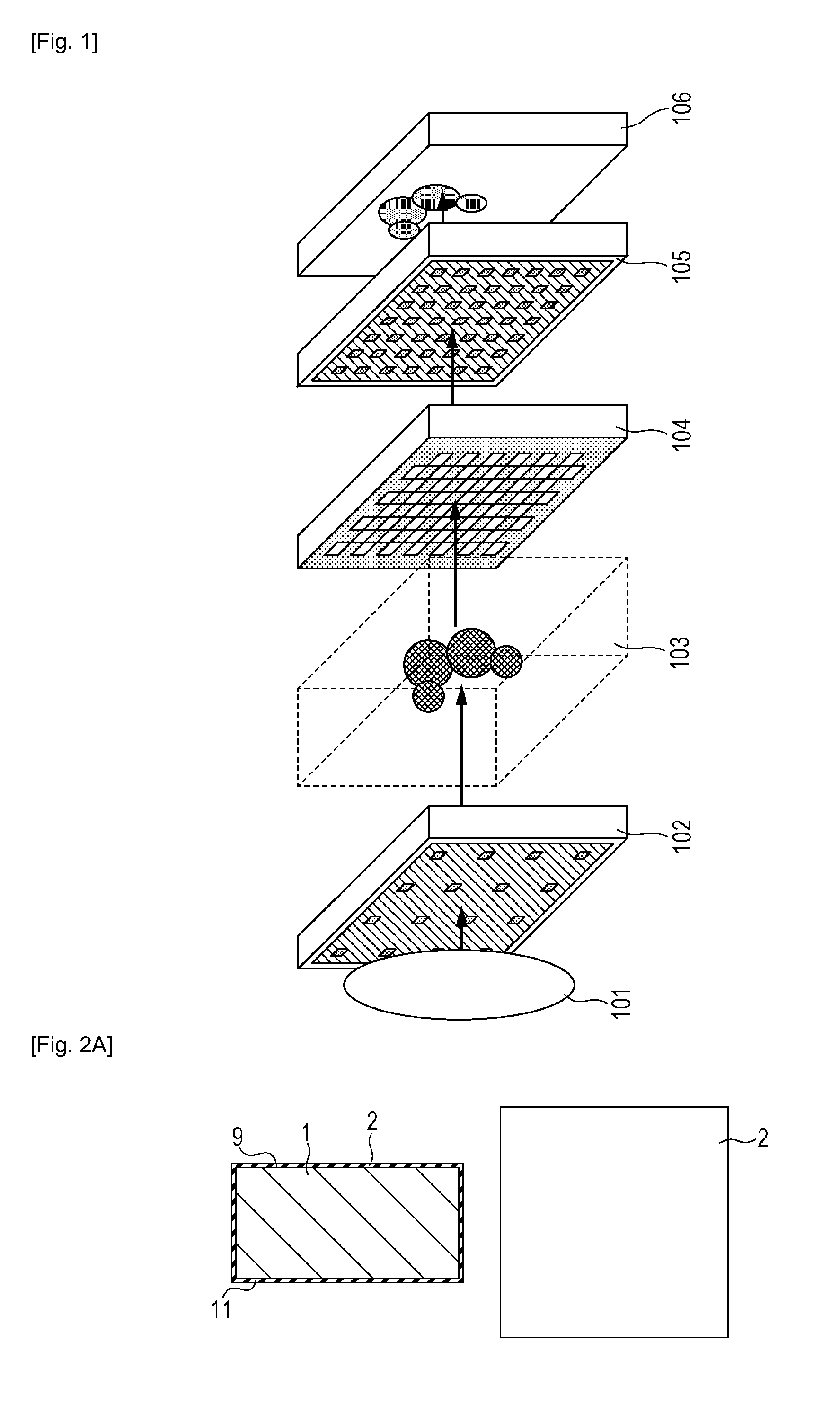
[0040]FIG. 1 is a schematic diagram of an imaging apparatus, in which a structure produced according to the present embodiment is used as a shield grating 105, to execute the X-ray Talbot interference method. The X-rays applied from an X-ray source 101 are limited to a predetermined size by a source grating 102 and are applied to an object 103. The X-rays passed through the object 103 are diffracted by a diffraction grating 104 and form an interference pattern on the shield grating 105. The shield grating 105 screens out part of the X-rays to form the interference pattern and form a moire. In this regard, the moire includes those having infinite or nearly infinite periods as well. The moire formed after passing through the...

second embodiment

[0082]In a second embodiment, a method for manufacturing a one-dimensional structure will be described. The one-dimensional structure produced according to the present embodiment can be used as a one-dimensional shield grating in the X-ray Talbot interference method.

[0083]The present embodiment is different from the first embodiment in that the pattern of the patterning of the mask is in the shape of a line, and the other steps are basically the same as the steps of the first embodiment. In this regard, in the one-dimensional structure, slit-shaped metal structures, which function as screen portions, are periodically arranged. Therefore, the present embodiment is different from the first embodiment in that a plurality of recessed portions are formed by etching the first surface of the silicon substrate, so as to form a mold, and a structure is produced by filling the metal into the plurality of recessed portions of the mold. Meanwhile, even when a recessed portion in which the end p...

third embodiment

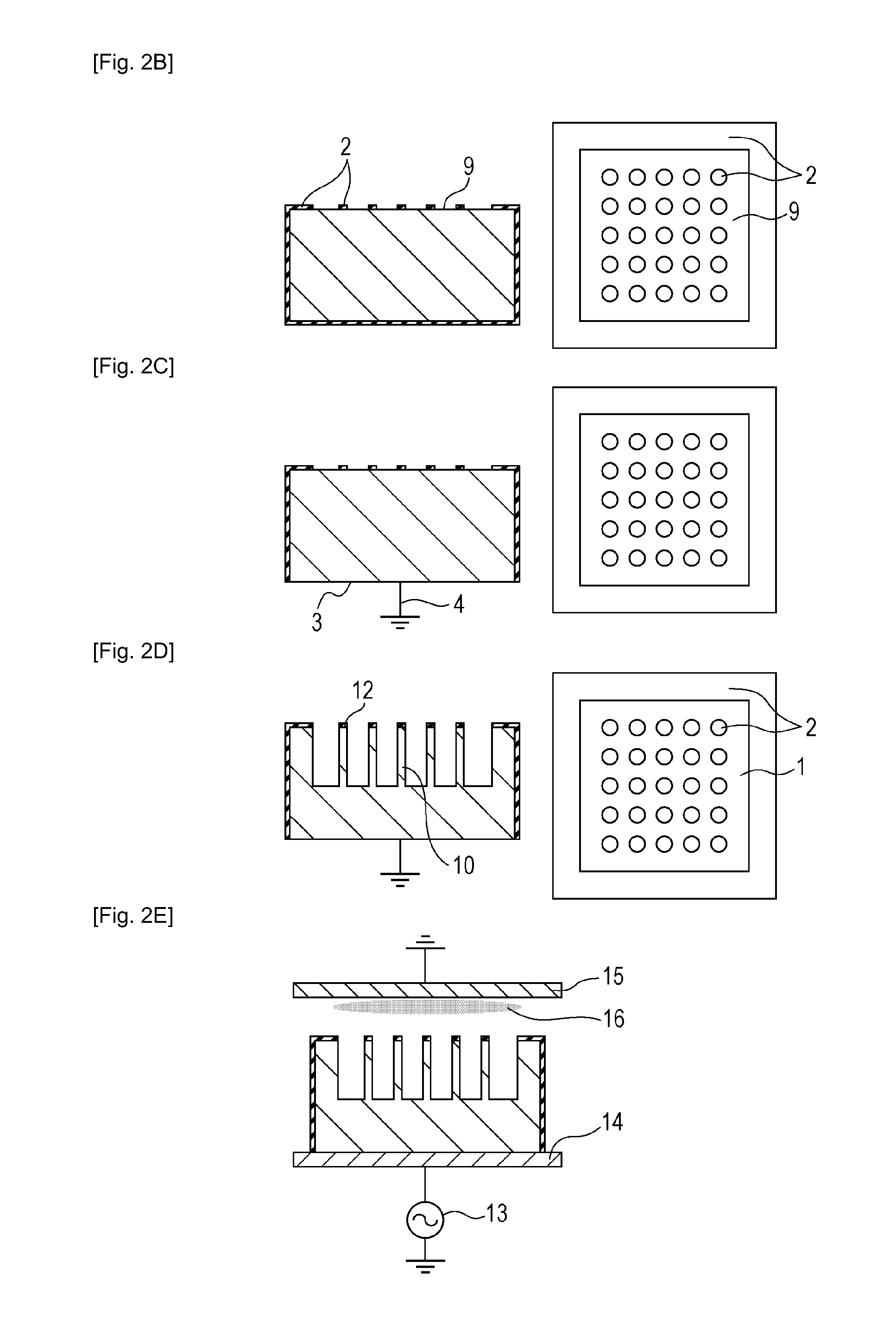
[0084]In a third embodiment, the mold and the structure produced according to the first embodiment will be described with reference to FIG. 3A to FIG. 3H. In the mold used for producing the structure of the present embodiment, a plurality of convex portions 10 are formed on the first surface 9 of the silicon substrate 1. It is desirable that the aspect ratios of the plurality of convex portions are 20 or more and 200 or less. An insulating film 7 made from an inorganic compound is formed on top surfaces 12 of the plurality of convex portions 10, and the insulating film 7 is formed on the portions excluding the bottom 19 between the plurality of convex portions. Silicon is exposed at the second surface 11 opposite to the first surface 9, and this portion, at which silicon is exposed, can be used as the electrically conductive opening. In performing the steps after the step to form the plurality of convex portions on the silicon substrate up to the step to fill the metal in between th...


PUM

PropertyMeasurementUnit
Lengthaaaaaaaaaa
Fractionaaaaaaaaaa
Fractionaaaaaaaaaa

Abstract

A method for manufacturing a structure by using a silicon mold, in which disturbances in arrangement due to charges are reduced, can be provided.The method for manufacturing a structure includes the steps of forming a recessed portion in a silicon substrate, cleaning, drying, or conveying the silicon substrate while charges of a plurality of portions sandwiched between the recessed portion are removed, and filling a metal into the recessed portion of the silicon substrate subjected to the cleaning, drying, or conveying.

Description

TECHNICAL FIELD[0001]The present invention relates to a structure. In particular, the present invention relates to a structure for an X-ray phase contrast imaging apparatus.BACKGROUND ART[0002]A grating made from a structure having a periodic structure is used as a spectral element for various apparatuses. In particular, a grating formed from a structure made from a metal having a high X-ray absorbance characteristic is used in the fields of the nondestructive inspection of objects and medical care.[0003]One purpose of the structure made from a metal having a high X-ray absorbance characteristic is a shield grating of an imaging apparatus to pick up an image by using X-ray Talbot interferometry. The imaging method by using the X-ray Talbot interferometry (X-ray Talbot interference method) is one of imaging methods (X-ray phase imaging methods) taking advantage of X-ray phase contrast.[0004]The X-ray Talbot interference method will be described briefly. In general imaging apparatus t...

Claims


Application Information

Patent Timeline
IPC IPC(8): G01N23/20C25D1/00
CPCC25D1/00G01N23/20A61B6/484G03F7/00G21K1/025G21K2207/005B81B3/0008B81C1/00952
Inventor SETOMOTO, YUTAKATESHIMA, TAKAYUKI
Owner CANON KK
Learn More