Variable capacitance element and high-frequency device

Active Publication Date: 2014-08-14
MURATA MFG CO LTD
View PDF4 Cites 22 Cited by
  • Summary
  • Abstract
  • Description
  • Claims
  • Application Information

AI Technical Summary

Benefits of technology

The patent text discusses a solution for designing a variable capacitance element and a high-frequency device. The solution includes a control voltage application circuit that addresses issues such as distortion, size, and circuit complexity. The technical effects of the patent text are improved reliability and performance of the device by eliminating distortion and ensuring impact resistance.

Problems solved by technology

However, it has become difficult to ensure an adequate antenna size as the terminals of late are increasingly downsized, and the antenna's bandwidth may not be broadened if the size of the antenna is small.
However, when a variable-capacitance diode and a switching circuit are provided, it is necessary to provide a space for mounting these active elements, and there is often a case in which the resonant frequency changes because distortion may easily occur since these elements are active elements.
Further, a large number of capacitors and switches are necessary in order to adjust the capacitance value in fine steps by switching between the plurality of capacitors.
This may adversely complicate the circuit architecture, and increase the size of an IC.
However, this may easily make an RFID device complicated and larger since mechanical control is required in order to change its capacitance value, and it is often not possible to ensure reliability on impact due to falling or the like.

Method used


Image

  • Variable capacitance element and high-frequency device
  • Variable capacitance element and high-frequency device
  • Variable capacitance element and high-frequency device

Examples


Embodiment Construction

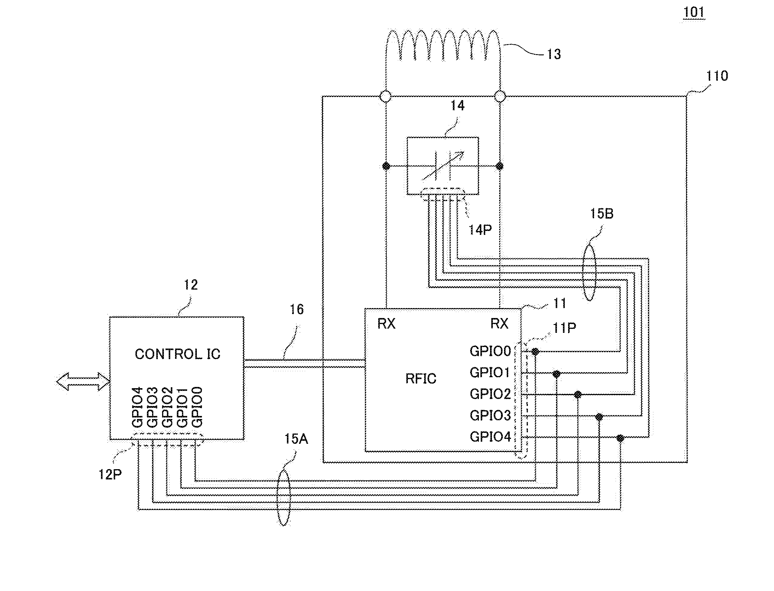
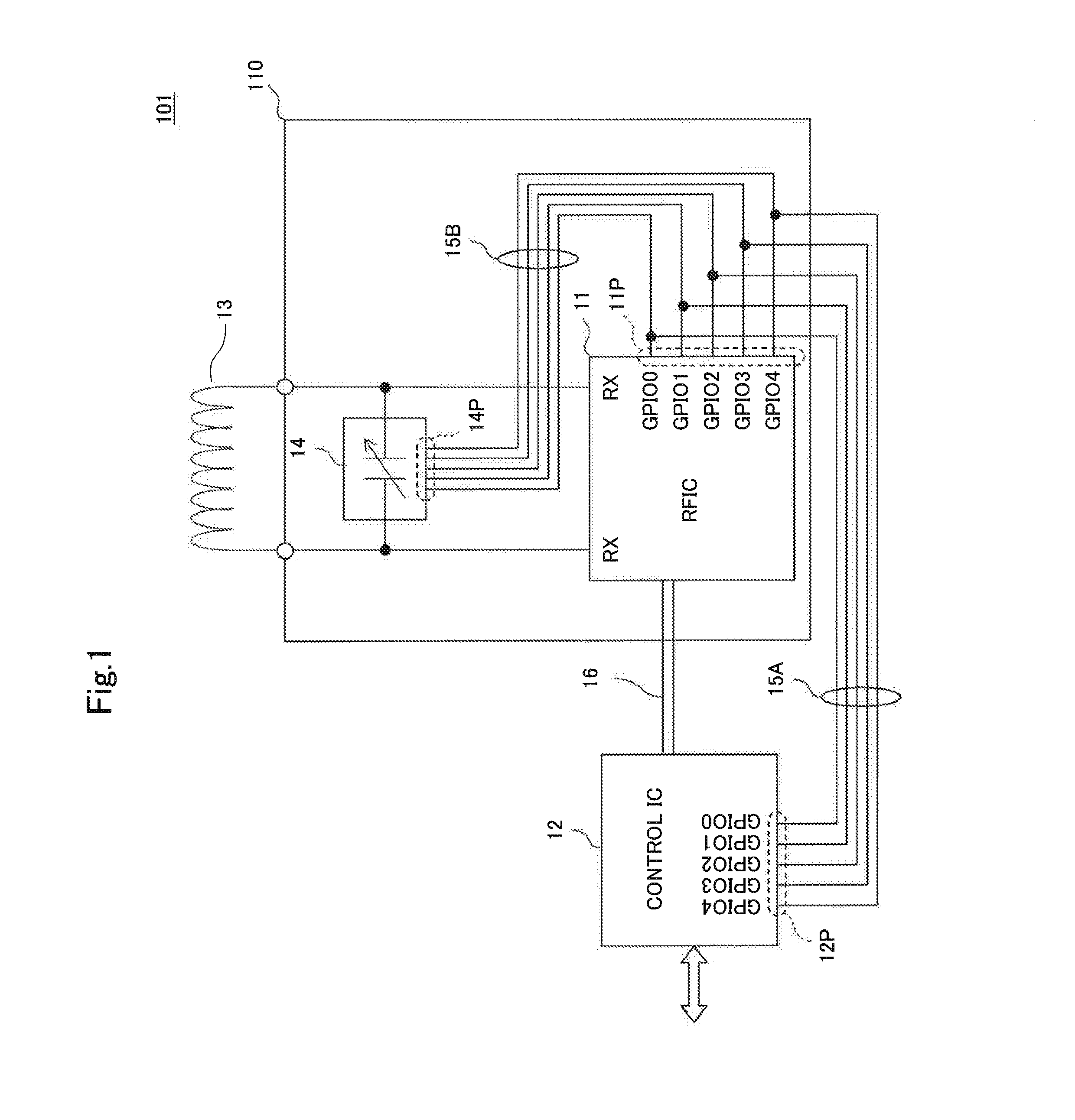
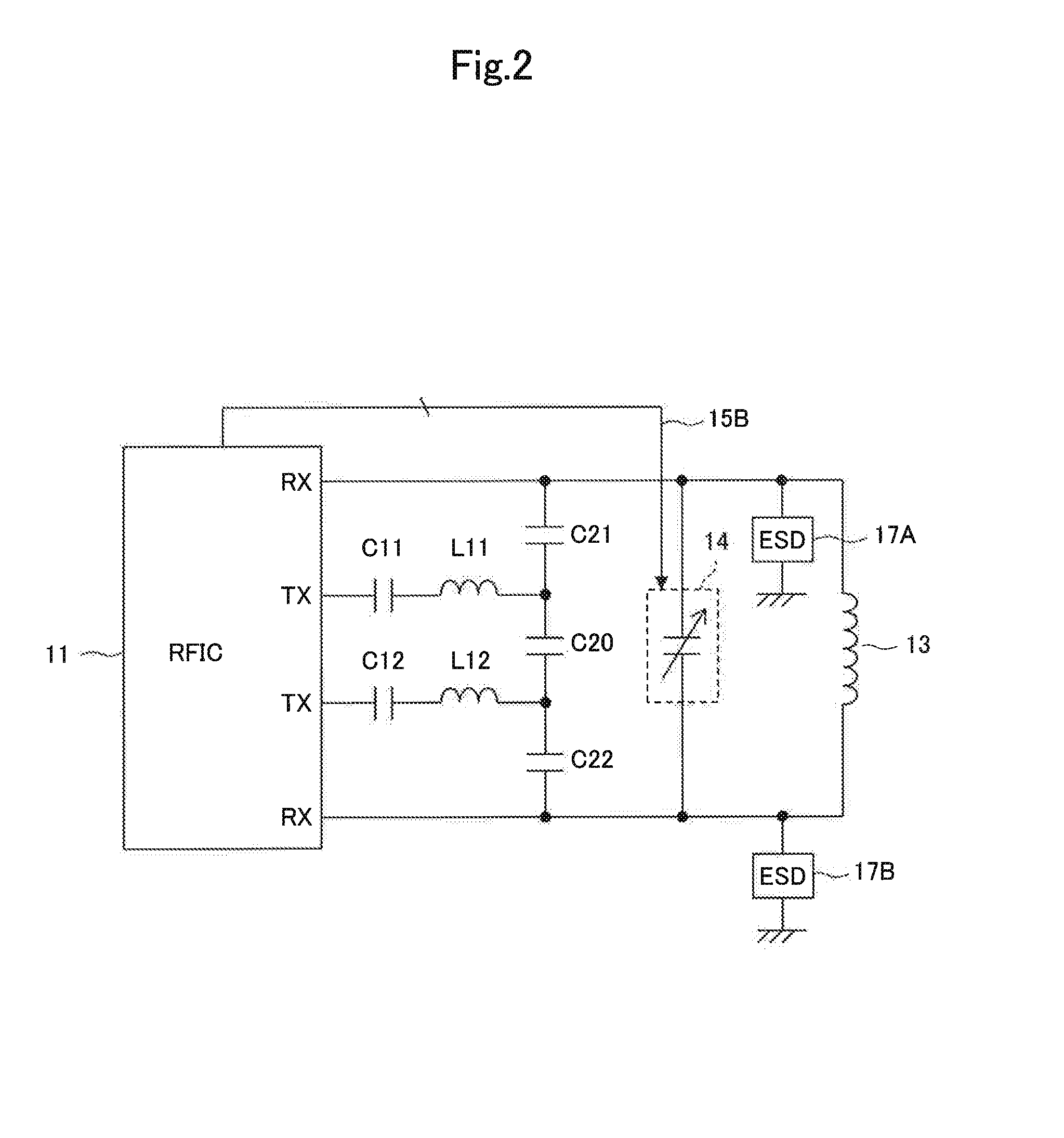
[0036]FIG. 1 is a circuit diagram of a communication circuit 101 including a variable capacitance element and a high-frequency device that include a control voltage application circuit. The communication circuit 101 is one example of NFC modules. The communication circuit 101 preferably includes an RFIC 11, a control IC 12, an antenna coil 13, and a variable capacitance element 14. The variable capacitance element 14 and the RFIC 11 constitute a variable-capacitance-element built-in RFIC 110. In the present preferred embodiment, the variable capacitance element 14 preferably is the variable capacitance element including a control voltage application circuit. A circuit configured by the variable-capacitance-element built-in RFIC 110 and the antenna coil 13 corresponds to a “high-frequency device” according to various preferred embodiments of the present invention.

[0037]The RFIC 11 includes IO terminals 11P for GPIO (General Purpose Input / Output). Similarly, the control IC 12 includes...


PUM


Abstract

A high-frequency device includes an antenna coil, a variable capacitance element, and an RFIC. The variable capacitance element is configured by capacitor units in each of which a ferroelectric film is sandwiched between capacitor electrodes, and a capacitance value changes according to a control voltage applied between the capacitor electrodes. A control voltage application circuit configured by a plurality of resistance elements of different resistance values, and a resistance element of the variable capacitance element unit configured to apply a control voltage to the variable capacitance element are arranged in a layered manner above the capacitor unit. Thus, a variable capacitance element and a high-frequency device that includes a control voltage application circuit eliminating problems such as distortion due to active elements and growing IC size along with complication of circuit architecture, and ensuring reliability on impact due to falling or the like, are provided.

Description

BACKGROUND OF THE INVENTION[0001]1. Field of the Invention[0002]The present invention relates to a variable capacitance element and a high-frequency device that include a control voltage application circuit preferably for use in an RFID (Radio Frequency Identification) system or a near field communication (NFC: Near Field Communication) system, in which communication with a target device is performed by an electromagnetic field signal.[0003]2. Description of the Related Art[0004]The NFC is one of near field communication standards using a frequency band of 13 MHz, and expected to be applied to various terminals including mobile communication terminals. A mobile communication terminal using NFC typically has an RFIC for NFC built in a main body of the terminal, and the RFIC for NFC is connected to an antenna coil for NFC that is also built within the terminal main body. Further, the antenna coil is connected to a capacitance element so as to resonate at a communication frequency, and...

Claims


Application Information

Patent Timeline
IPC IPC(8): H01Q7/00G06K7/10G06K19/077H01G7/00H01Q5/10
CPCH01Q7/005G06K19/07779G06K7/10336H01G7/00H01Q1/2225H01Q1/243H04B5/77H04B5/26G06K19/0726H01G7/06H04B5/48G06K19/07G06K19/077H01Q5/10
Inventor IKEMOTO, NOBUONAKAISO, TOSHIYUKITANIGUCHI, KATSUMIGOUCHI, NAOKIIKEDA, NAOTO
Owner MURATA MFG CO LTD
Why Eureka
Try Eureka