Semiconductor device

Active Publication Date: 2014-08-21
SEMICON ENERGY LAB CO LTD
View PDF6 Cites 23 Cited by
  • Summary
  • Abstract
  • Description
  • Claims
  • Application Information

AI Technical Summary

Benefits of technology

[0023]According to one embodiment of the present invention, a semiconductor device can be provided in which deterioration of electrical characteristics which becomes more noticeable as the transistor is miniaturized can be suppressed. Alternatively, a semiconductor device with low power consumption can be provided. Alternatively, a highly reliable semiconductor device can be provided. Alternatively, a semiconductor device in which a lowerin

Problems solved by technology

When the threshold voltage is lowered, a current at which the gate voltage is 0V (the current is also referred to as Icut) is increased, which might lead to an increase of power consumption of a semiconductor device or the l

Method used


Image

  • Semiconductor device
  • Semiconductor device
  • Semiconductor device

Examples


Example

Embodiment 1

[0064]In this embodiment, an example of a semiconductor device (memory device) which can hold stored data even when not powered, and which has an unlimited number of write cycles will be described with reference to drawings.

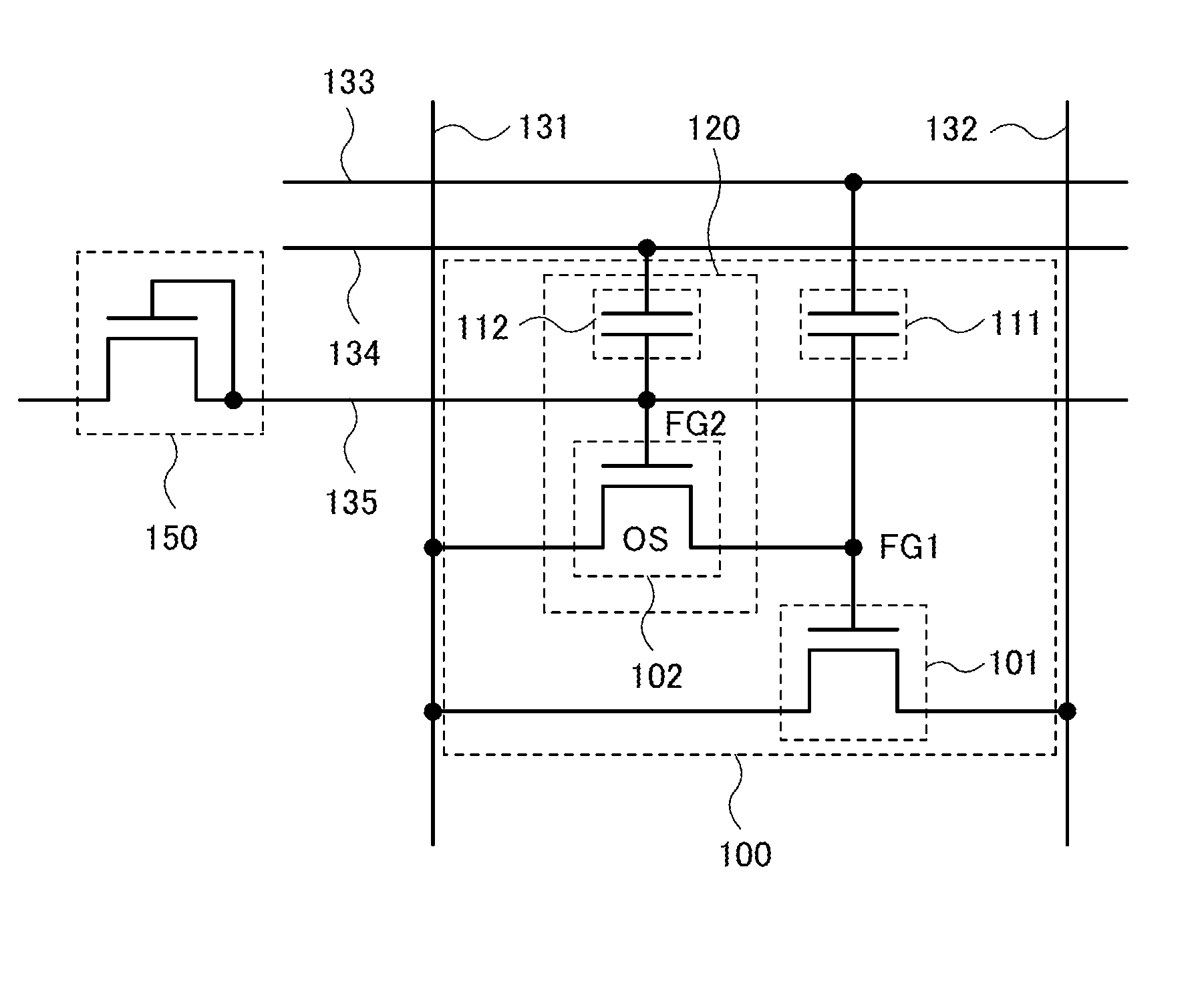
[0065]FIG. 1 is a circuit diagram of a semiconductor device of one embodiment of the present invention.

[0066]A semiconductor device 100 illustrated in FIG. 1 includes a first transistor 101, a second transistor 102, a first capacitor 111, and a second capacitor 112. One of a source electrode and a drain electrode of the first transistor 101 is electrically connected to a first wiring 131, the other of the source electrode and the drain electrode of the first transistor is electrically connected to a second wiring 132, and a gate electrode of the first transistor is electrically connected to one of a source electrode and a drain electrode of the second transistor 102 and one of electrodes of the first capacitor 111. The other of the source electrode an...

Example

Embodiment 2

[0095]In this embodiment, a semiconductor device which can hold stored data even when not powered, which does not have a limitation on the number of write cycles, and which has a structure different from the structure described in Embodiment 1 will be described.

[0096]FIG. 6 is a circuit diagram of a semiconductor device of one embodiment of the present invention.

[0097]A semiconductor device 200 illustrated in FIG. 6 includes a transistor 201, a first capacitor 211, and a second capacitor 212. One of a source electrode and a drain electrode of the transistor 201 is electrically connected to a first wiring 231, the other of the source electrode and the drain electrode is electrically connected to one of electrodes of the first capacitor 211, and a gate electrode of the transistor is electrically connected to one of electrodes of the second capacitor 212 and a fifth wiring 235. The other electrode of the first capacitor 211 is electrically connected to a second wiring 232, ...

Example

Embodiment 3

[0117]In this embodiment, a semiconductor device (display device) to which one embodiment of the present invention can be applied will be described.

[0118]As a display element provided in the display device, a liquid crystal element (also referred to as a liquid crystal display element), a light-emitting element (also referred to as a light-emitting display element), or the like can be used. The light-emitting element includes, in its category, an element whose luminance is controlled by current or voltage, specifically an inorganic electroluminescent (EL) element, an organic EL element, and the like. Furthermore, a display medium whose contrast is changed by an electric effect, such as electronic ink, can be used as the display element. A display device including an EL element and a display device including a liquid crystal element are described below as examples of the display device.

[0119]The display device described below includes, in its category, a panel in which a ...


PUM


Abstract

The semiconductor device of the present invention comprises first and second transistors and first and second capacitors. One of source and drain electrodes of the first transistor is electrically connected to a first wiring, the other is electrically connected to a second wiring, and a gate electrode of the first transistor is electrically connected to one of a source electrode and a drain electrode of the second transistor and one of electrodes of the first capacitor. The other of the source and drain electrodes of the second transistor is electrically connected to the first wiring, and a gate electrode of the second transistor is electrically connected to one of electrodes of a second capacitor and a fifth wiring. The other electrode of the first capacitor is electrically connected to a third wiring, and the other electrode of the second capacitor is eclectically connected to a fourth wiring.

Description

BACKGROUND OF THE INVENTION[0001]1. Field of the Invention[0002]The present invention relates to an object, a method, or a manufacturing method. In addition, the present invention relates to a process, a machine, manufacture, or a composition of matter. In particular, the present invention relates to, for example, a semiconductor device, a display device, a light-emitting device, a power storage device, a driving method thereof, or a manufacturing method thereof. The present invention particularly relates to a semiconductor device, a display device, or a light-emitting device each including an oxide semiconductor, for example.[0003]In this specification, a semiconductor device generally means a device which can function by utilizing semiconductor characteristics. An electro-optical device, a semiconductor circuit, and an electric device may be included in a semiconductor device or may include a semiconductor device.[0004]2. Description of the Related Art[0005]Attention has been focu...

Claims


Application Information

Patent Timeline
IPC IPC(8): H01L29/786H01L29/24H01L27/06
CPCH01L29/7869H01L29/24H01L27/0629H01L27/1225H01L27/1255H01L27/105H01L27/1207H01L29/16H01L29/78
Inventor MATSUBAYASHI, DAISUKE
Owner SEMICON ENERGY LAB CO LTD
Why Eureka
Try Eureka